参数资料
| 型号: | MX7705EUE+ |
| 厂商: | Maxim Integrated Products |
| 文件页数: | 15/33页 |
| 文件大小: | 0K |
| 描述: | IC ADC 16BIT 2CH 16-TSSOP |
| 产品培训模块: | MAX11200 ADC Lead (SnPb) Finish for COTS Obsolescence Mitigation Program |
| 标准包装: | 96 |
| 位数: | 16 |
| 采样率(每秒): | 500 |
| 数据接口: | MICROWIRE?,QSPI?,串行,SPI? |
| 转换器数目: | 1 |
| 功率耗散(最大): | 755mW |
| 电压电源: | 单电源 |
| 工作温度: | -40°C ~ 85°C |
| 安装类型: | 表面贴装 |
| 封装/外壳: | 16-TSSOP(0.173",4.40mm 宽) |
| 供应商设备封装: | 16-TSSOP |
| 包装: | 管件 |
| 输入数目和类型: | 2 个差分,单极 |
第1页第2页第3页第4页第5页第6页第7页第8页第9页第10页第11页第12页第13页第14页当前第15页第16页第17页第18页第19页第20页第21页第22页第23页第24页第25页第26页第27页第28页第29页第30页第31页第32页第33页
MX7705
Communications Register
The byte-wide communications register is bidirectional
so it can be written and read. The byte written to the
communications register indicates the next read or write
operation on the selected register, the power-down
mode, and the analog input channel (Table 6). The
DRDY bit indicates the conversion status.
0/DRDY: (Default = 0) Communication-Start/Data-Ready
Bit. Write a 0 to the 0/DRDY bit to start a write operation to
the communications register. If 0/DRDY = 1, then the
device waits until a 0 is written to 0/DRDY before continu-
ing to load the remaining bits. For a read operation, the
0/DRDY bit shows the status of the conversion. The
DRDY bit returns a 0 if the conversion is complete and
the data is ready. DRDY returns a 1 if the new data has
been read and the next conversion is not yet complete. It
has the same value as the DRDY output pin.
RS2, RS1, RS0: (Default = 0, 0, 0) Register-Select Bits.
RS0, RS1, and RS2 select the next register to be
accessed as shown in Table 7.
R/
W: (Default = 0) Read-/Write-Select Bit. Use this bit to
select if the next register access is a read or a write
operation. Set R/W = 0 to select a write operation or set
R/W = 1 for a read operation on the selected register.
PD: (Default = 0) Power-Down Control Bit. Set PD = 1
to initiate power-down mode. Set PD = 0 to take the
device out of power-down mode. If CLKDIS = 0, CLKOUT
remains active during power-down mode to provide a
clock source for other devices in the system.
CH0, CH1: (Default = 0, 0) Channel-Select Bit. Write to
the CH0 and CH1 bits to select the conversion channel or
to access the calibration data shown in Table 8. The cali-
bration coefficients of a particular channel are stored in
one of the three offset and gain-register pairs in Table 8.
Set CH1 = 1 and CH0 = 0 to evaluate the noise perfor-
mance of the part without external noise sources. In this
noise evaluation mode, connect AIN1- to an external volt-
age within the allowable common-mode range.
Setup Register
The byte-wide setup register is bidirectional, so it can
be written and read. The byte written to the setup regis-
ter sets the calibration modes, PGA gain, unipolar/bipo-
lar mode, buffer enable, and conversion start (Table 9).
MD1, MD0: (Default = 0, 0) Mode-Select Bits. See
Table 10 for normal operating mode, self-calibration,
zero-scale calibration, or full-scale calibration-mode
selection.
G2, G1, G0: (Default = 0, 0, 0) Gain-Selection Bits. See
Table 11 for PGA gain settings.
B/U: (Default = 0) Bipolar/Unipolar Mode Selection. Set
B/U = 0 to select bipolar mode. Set B/U = 1 to select
unipolar mode.
BUF: (Default = 0) Buffer-Enable Bit. For unbuffered
mode, disable the internal buffer of the MX7705 to reduce
power consumption by writing a 0 to the BUF bit. Write a
1 to this bit to enable the buffer. Use the internal buffer
when acquiring high source-impedance input signals.
FSYNC:
(Default
=
1)
Filter-Synchronization/
Conversion-Start Bit. Set FSYNC = 0 to begin calibration
or conversion. The MX7705 performs free-running con-
versions while FSYNC = 0. Set FSYNC = 1 to stop con-
verting data and to hold the nodes of the digital filter, the
filter-control logic, the calibration-control logic, and the
analog modulator in a reset state. The DRDY output does
not reset high if it is low (indicating that valid data has not
yet been read from the data register) when FSYNC goes
high. To clear the DRDY output, read the data register.
Clock Register
The byte-wide clock register is bidirectional, so it can
be written and read. The byte written to the setup regis-
ter sets the clock, filter first-notch frequency, and the
output data rate (Table 12).
MXID: (Default = 1) Maxim-Identifier Bit. This is a read-
only bit. Values written to this bit are ignored.
16-Bit, Low-Power, 2-Channel,
Sigma-Delta ADC
22
______________________________________________________________________________________
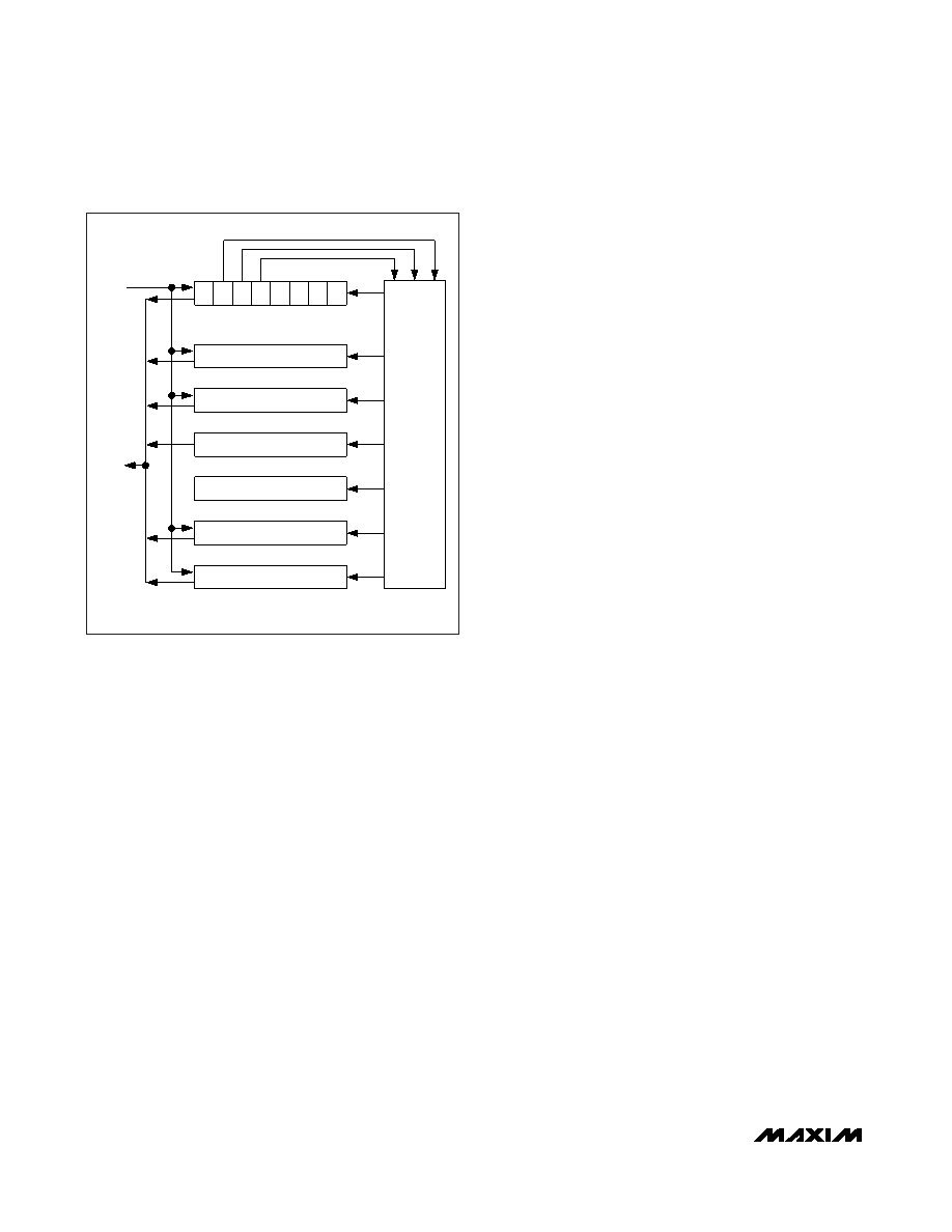
SETUP REGISTER (8 BITS)
RS2 RS1 RS0
CLOCK REGISTER (8 BITS)
DATA REGISTER (16 BITS)
TEST REGISTER (8 BITS)*
OFFSET REGISTER (24 BITS)
GAIN REGISTER (24 BITS)
COMMUNICATIONS REGISTER
REGISTER
SELECT
DECODER
DIN
DOUT
*THE TEST REGISTER IS USED FOR FACTORY TESTING ONLY.
Figure 10. Register Summary
相关PDF资料 |
PDF描述 |
|---|---|
| VI-B6Z-IU-F3 | CONVERTER MOD DC/DC 2V 80W |
| VI-B6Z-IU-F2 | CONVERTER MOD DC/DC 2V 80W |
| MAX1185ECM/V+ | IC ADC 10BIT 20MSPS DL LP 48TQFP |
| MS27497T16F99PB | CONN RCPT 23POS WALL MNT W/PINS |
| IDT723644L12PF8 | IC FIFO SYNC 2048X36 128QFP |
相关代理商/技术参数 |
参数描述 |
|---|---|
| MX7705EUE+ | 功能描述:模数转换器 - ADC 16-Bit 2Ch Precision ADC RoHS:否 制造商:Texas Instruments 通道数量:2 结构:Sigma-Delta 转换速率:125 SPs to 8 KSPs 分辨率:24 bit 输入类型:Differential 信噪比:107 dB 接口类型:SPI 工作电源电压:1.7 V to 3.6 V, 2.7 V to 5.25 V 最大工作温度:+ 85 C 安装风格:SMD/SMT 封装 / 箱体:VQFN-32 |
| MX7705EUE+T | 功能描述:模数转换器 - ADC 16-Bit 2Ch Precision ADC RoHS:否 制造商:Texas Instruments 通道数量:2 结构:Sigma-Delta 转换速率:125 SPs to 8 KSPs 分辨率:24 bit 输入类型:Differential 信噪比:107 dB 接口类型:SPI 工作电源电压:1.7 V to 3.6 V, 2.7 V to 5.25 V 最大工作温度:+ 85 C 安装风格:SMD/SMT 封装 / 箱体:VQFN-32 |
| MX7705EUE-T | 功能描述:模数转换器 - ADC RoHS:否 制造商:Texas Instruments 通道数量:2 结构:Sigma-Delta 转换速率:125 SPs to 8 KSPs 分辨率:24 bit 输入类型:Differential 信噪比:107 dB 接口类型:SPI 工作电源电压:1.7 V to 3.6 V, 2.7 V to 5.25 V 最大工作温度:+ 85 C 安装风格:SMD/SMT 封装 / 箱体:VQFN-32 |
| MX7705EWE | 功能描述:模数转换器 - ADC RoHS:否 制造商:Texas Instruments 通道数量:2 结构:Sigma-Delta 转换速率:125 SPs to 8 KSPs 分辨率:24 bit 输入类型:Differential 信噪比:107 dB 接口类型:SPI 工作电源电压:1.7 V to 3.6 V, 2.7 V to 5.25 V 最大工作温度:+ 85 C 安装风格:SMD/SMT 封装 / 箱体:VQFN-32 |
| MX7705EWE+ | 功能描述:模数转换器 - ADC 16-Bit 2Ch Precision ADC RoHS:否 制造商:Texas Instruments 通道数量:2 结构:Sigma-Delta 转换速率:125 SPs to 8 KSPs 分辨率:24 bit 输入类型:Differential 信噪比:107 dB 接口类型:SPI 工作电源电压:1.7 V to 3.6 V, 2.7 V to 5.25 V 最大工作温度:+ 85 C 安装风格:SMD/SMT 封装 / 箱体:VQFN-32 |
发布紧急采购,3分钟左右您将得到回复。