- 您现在的位置:买卖IC网 > PDF目录189003 > NAND08GR3B3BZC6E (STMICROELECTRONICS) 1G X 8 FLASH 1.8V PROM, 35 ns, PBGA63 PDF资料下载
参数资料
| 型号: | NAND08GR3B3BZC6E |
| 厂商: | STMICROELECTRONICS |
| 元件分类: | PROM |
| 英文描述: | 1G X 8 FLASH 1.8V PROM, 35 ns, PBGA63 |
| 封装: | 9.50 X 12 MM, 1.40 MM HEIGHT, 0.80 MM PITCH, ROHS COMPLIANT, LFBGA-63 |
| 文件页数: | 19/59页 |
| 文件大小: | 998K |
| 代理商: | NAND08GR3B3BZC6E |
第1页第2页第3页第4页第5页第6页第7页第8页第9页第10页第11页第12页第13页第14页第15页第16页第17页第18页当前第19页第20页第21页第22页第23页第24页第25页第26页第27页第28页第29页第30页第31页第32页第33页第34页第35页第36页第37页第38页第39页第40页第41页第42页第43页第44页第45页第46页第47页第48页第49页第50页第51页第52页第53页第54页第55页第56页第57页第58页第59页
NAND512-B, NAND01G-B, NAND02G-B, NAND04G-B, NAND08G-B
26/59
Cache Program
The Cache Program operation is used to improve
the programming throughput by programming
data using the Cache Register. The Cache Pro-
gram operation can only be used within one block.
The Cache Register allows new data to be input
while the previous data that was transferred to the
Page Buffer is programmed into the memory ar-
ray.
Each Cache Program operation consists of five
steps (refer to Figure 16.):
1.
First of all the program setup command is
issued (one bus cycle to issue the program
setup command then four bus write cycles to
input the address), the data is then input (up to
2112 Bytes/ 1056 Words) and loaded into the
Cache Register.
2.
One bus cycle is required to issue the confirm
command to start the P/E/R Controller.
3.
The P/E/R Controller then transfers the data to
the Page Buffer. During this the device is busy
for a time of tWHBH2.
4.
Once the data is loaded into the Page Buffer
the P/E/R Controller programs the data into
the memory array. As soon as the Cache
Registers are empty (after tWHBH2) a new
Cache program command can be issued,
while the internal programming is still
executing.
Once the program operation has started the Sta-
tus Register can be read using the Read Status
Register command. During Cache Program oper-
ations SR5 can be read to find out whether the in-
ternal programming is ongoing (SR5 = ‘0’) or has
completed (SR5 = ‘1’) while SR6 indicates wheth-
er the Cache Register is ready to accept new data.
If any errors have been detected on the previous
page (Page N-1), the Cache Program Error Bit SR1
will be set to ‘1', while if the error has been detect-
ed on Page N the Error Bit SR0 will be set to '1’.
When the next page (Page N) of data is input with
the Cache Program command, tWHBH2 is affected
by the pending internal programming. The data will
only be transferred from the Cache Register to the
Page Buffer when the pending program cycle is
finished and the Page Buffer is available.
If the system monitors the progress of the opera-
tion using only the Ready/Busy signal, the last
page of data must be programmed with the Page
Program confirm command (10h).
If the Cache Program confirm command (15h) is
used instead, Status Register bit SR5 must be
polled to find out if the last programming is finished
before starting any other operations.
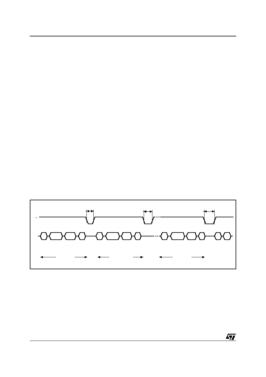
Figure 16. Cache Program Operation
Note: 1. Up to 64 pages can be programmed in one Cache Program operation.
2. tCACHEPG is the program time for the last page + the program time for the (last 1)
th page
(Program command cycle time + Last
page data loading time).
I/O
RB
Address
Inputs
ai08672
80h
Page
Program
Code
Read Status
Register
Busy
Data
Inputs
15h
Cache
Program
Code
80h
Page
Program
Code
15h
Cache Program
Confirm Code
Busy
Last Page
tBLBH5
(Cache Busy time)
tBLBH5
tCACHEPG
SR0
70h
80h
10h
Page
Program
Confirm Code
Busy
First Page
Second Page
(can be repeated up to 63 times)
Address
Inputs
Data
Inputs
Address
Inputs
Data
Inputs
相关PDF资料 |
PDF描述 |
|---|---|
| NAND08GR3B3CN1E | 1G X 8 FLASH 1.8V PROM, 35 ns, PDSO48 |
| NAND08GW4B2CZC1F | 512M X 16 FLASH 3V PROM, 35 ns, PBGA63 |
| NAND08GW4B3AZC6 | 512M X 16 FLASH 3V PROM, 35 ns, PBGA63 |
| NAND08GW4B3BN1T | 512M X 16 FLASH 3V PROM, 35 ns, PDSO48 |
| NAND08GW4B3BN6E | 512M X 16 FLASH 3V PROM, 35 ns, PDSO48 |
相关代理商/技术参数 |
参数描述 |
|---|---|
| NAND08GR3B4CZL6E | 制造商:Micron Technology Inc 功能描述:NAND - Trays |
| NAND08GR3B4CZL6F | 制造商:Micron Technology Inc 功能描述:NAND - Tape and Reel |
| NAND08GW3B2AN6E | 功能描述:闪存 4 GBit 2112 Byte 1056 WP 1.8v/3v RoHS:否 制造商:ON Semiconductor 数据总线宽度:1 bit 存储类型:Flash 存储容量:2 MB 结构:256 K x 8 定时类型: 接口类型:SPI 访问时间: 电源电压-最大:3.6 V 电源电压-最小:2.3 V 最大工作电流:15 mA 工作温度:- 40 C to + 85 C 安装风格:SMD/SMT 封装 / 箱体: 封装:Reel |
| NAND08GW3B2AN6F | 功能描述:闪存 4 GB 2112B 1056 Word Pg 1.8V/3V RoHS:否 制造商:ON Semiconductor 数据总线宽度:1 bit 存储类型:Flash 存储容量:2 MB 结构:256 K x 8 定时类型: 接口类型:SPI 访问时间: 电源电压-最大:3.6 V 电源电压-最小:2.3 V 最大工作电流:15 mA 工作温度:- 40 C to + 85 C 安装风格:SMD/SMT 封装 / 箱体: 封装:Reel |
| NAND08GW3B2BN6E | 制造商:Micron Technology Inc 功能描述:NAND & S.MEDIA FLASH - Trays |
发布紧急采购,3分钟左右您将得到回复。