- 您现在的位置:买卖IC网 > PDF目录8676 > NB100EP223FAR2G (ON Semiconductor)IC CLOCK BUFFER MUX 2:22 64-LQFP PDF资料下载
参数资料
| 型号: | NB100EP223FAR2G |
| 厂商: | ON Semiconductor |
| 文件页数: | 1/10页 |
| 文件大小: | 0K |
| 描述: | IC CLOCK BUFFER MUX 2:22 64-LQFP |
| 标准包装: | 1,500 |
| 系列: | 100EP |
| 类型: | 扇出缓冲器(分配),多路复用器 |
| 电路数: | 1 |
| 比率 - 输入:输出: | 2:22 |
| 差分 - 输入:输出: | 是/是 |
| 输入: | HSTL,LVDS,LVPECL |
| 输出: | HSTL |
| 频率 - 最大: | 500MHz |
| 电源电压: | 3 V ~ 3.6 V |
| 工作温度: | 0°C ~ 85°C |
| 安装类型: | 表面贴装 |
| 封装/外壳: | 64-LQFP 裸露焊盘 |
| 供应商设备封装: | 64-LQFP(10x10) |
| 包装: | 带卷 (TR) |
| 其它名称: | NB100EP223FAR2GOS |
Semiconductor Components Industries, LLC, 2006
November, 2006 Rev. 7
1
Publication Order Number:
NB100EP223/D
NB100EP223
3.3V1:22 Differential
HSTL/PECL to HSTL Clock
Driver with LVTTL Clock
Select and Output Enable
Description
The NB100EP223 is a low skew 1to22 differential clock driver,
designed with clock distribution in mind, accepting two clock sources
into an input multiplexer. The part is designed for use in low voltage
applications which require a large number of outputs to drive precisely
aligned low skew signals to their destination. The two clock inputs are
differential HSTL or LVPECL and they are selected by the CLK_SEL
pin which is LVTTL. To avoid generation of a runt clock pulse when
the device is enabled/disabled, the Output Enable (OE), which is
LVTTL, is synchronous ensuring the outputs will only be
enabled/disabled when they are already in LOW state (See Figure 7).
The NB100EP223 guarantees low outputtooutput skew. The
optimal design, layout, and processing minimize skew within a device
and from lot to lot. In any differential output pair, the same bias and
termination scheme is required. Unused output pairs should be left
unterminated (open) to “reduce power and switching noise as much as
possible.” Any unused single line of a differential pair should be
terminated the same as the used line to maintain balanced loads on the
differential driver outputs. The output structure uses an open emitter
architecture and will be terminated with 50
W to ground instead of a
standard HSTL configuration (See Figure 6). The wide VIHCMR
specification allows both pair of CLOCK inputs to accept LVDS
levels.
Features
100 ps Typical DevicetoDevice Skew
25 ps Typical Within Device Skew
HSTL Compatible Outputs Drive 50 W to Ground With No
Offset Voltage
Maximum Frequency >500 MHz
1 ns Typical Propagation Delay
LVPECL and HSTL Mode Operating Range: VCC = 3 V to 3.6 V
with GND = 0 V, VCCO = 1.6 V to 2.0 V
Q Output will Default Low with Inputs Open
Thermally Enhanced 64Lead LQFP
CLOCK Inputs are LVDSCompatible; Requires External 100 W
LVDS Termination Resistor
PbFree Packages are Available*
*For additional information on our PbFree strategy and soldering details, please
download the ON Semiconductor Soldering and Mounting Techniques
Reference Manual, SOLDERRM/D.
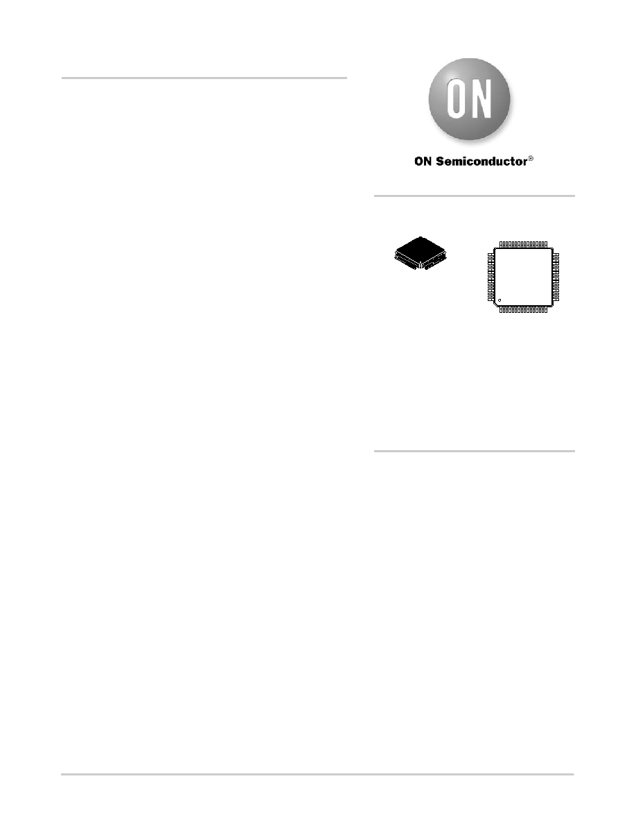
LQFP64
FA SUFFIX
CASE 848G
MARKING
DIAGRAM*
*For additional marking information, refer to
Application Note AND8002/D.
http://onsemi.com
See detailed ordering and shipping information in the package
dimensions section on page 8 of this data sheet.
ORDERING INFORMATION
A
= Assembly Location
WL
= Wafer Lot
YY
= Year
WW
= Work Week
G= PbFree Package
NB100
EP223
AWLYYWWG
64
1
相关PDF资料 |
PDF描述 |
|---|---|
| V300A36H500BF2 | CONVERTER MOD DC/DC 36V 500W |
| SY100E111LEJC TR | IC CLK FANOUT BUFFER 1:9 28-PLCC |
| AD9760ARZ50RL | IC DAC 10BIT 125MSPS 28TSSOP |
| V300A36H500BF | CONVERTER MOD DC/DC 36V 500W |
| SY100E111LEJC | IC CLK FANOUT BUFFER 1:9 28-PLCC |
相关代理商/技术参数 |
参数描述 |
|---|---|
| NB100LVEP17 | 制造商:ONSEMI 制造商全称:ON Semiconductor 功能描述:2.5V / 3.3V Quad Differential Driver/Receiver |
| NB100LVEP17/D | 制造商:未知厂家 制造商全称:未知厂家 功能描述:2.5V / 3.3V ECL Quad Differential Driver/Receiver |
| NB100LVEP17DT | 功能描述:总线接收器 2.5V/3.3V/5V ECL RoHS:否 制造商:Texas Instruments 接收机数量:4 接收机信号类型:Differential 接口类型:EIA/TIA-422-B, V.11 工作电源电压:3.3 V 最大工作温度:+ 85 C 最小工作温度:- 40 C 封装 / 箱体:TSSOP-16 封装:Reel |
| NB100LVEP17DTG | 功能描述:总线接收器 2.5V/3.3V/5V ECL Quad Diff Driver RoHS:否 制造商:Texas Instruments 接收机数量:4 接收机信号类型:Differential 接口类型:EIA/TIA-422-B, V.11 工作电源电压:3.3 V 最大工作温度:+ 85 C 最小工作温度:- 40 C 封装 / 箱体:TSSOP-16 封装:Reel |
| NB100LVEP17DTR2 | 功能描述:总线接收器 2.5V/3.3V/5V ECL RoHS:否 制造商:Texas Instruments 接收机数量:4 接收机信号类型:Differential 接口类型:EIA/TIA-422-B, V.11 工作电源电压:3.3 V 最大工作温度:+ 85 C 最小工作温度:- 40 C 封装 / 箱体:TSSOP-16 封装:Reel |
发布紧急采购,3分钟左右您将得到回复。