- 您现在的位置:买卖IC网 > PDF目录8676 > NB100EP223FAR2G (ON Semiconductor)IC CLOCK BUFFER MUX 2:22 64-LQFP PDF资料下载
参数资料
| 型号: | NB100EP223FAR2G |
| 厂商: | ON Semiconductor |
| 文件页数: | 8/10页 |
| 文件大小: | 0K |
| 描述: | IC CLOCK BUFFER MUX 2:22 64-LQFP |
| 标准包装: | 1,500 |
| 系列: | 100EP |
| 类型: | 扇出缓冲器(分配),多路复用器 |
| 电路数: | 1 |
| 比率 - 输入:输出: | 2:22 |
| 差分 - 输入:输出: | 是/是 |
| 输入: | HSTL,LVDS,LVPECL |
| 输出: | HSTL |
| 频率 - 最大: | 500MHz |
| 电源电压: | 3 V ~ 3.6 V |
| 工作温度: | 0°C ~ 85°C |
| 安装类型: | 表面贴装 |
| 封装/外壳: | 64-LQFP 裸露焊盘 |
| 供应商设备封装: | 64-LQFP(10x10) |
| 包装: | 带卷 (TR) |
| 其它名称: | NB100EP223FAR2GOS |
NB100EP223
http://onsemi.com
7
APPLICATIONS INFORMATION
Using the thermally enhanced package of the
NB100EP223
The NB100EP223 uses a thermally enhanced 64lead
LQFP package. The package is molded so that a portion of
the leadframe is exposed at the surface of the package
bottom side. This exposed metal pad will provide the low
thermal impedance that supports the power consumption of
the NB100EP223 highspeed bipolar integrated circuit and
will ease the power management task for the system design.
In multilayer board designs, a thermal land pattern on the
printed circuit board and thermal vias are recommended to
maximize both the removal of heat from the package and
electrical performance of the NB100EP223. The size of the
land pattern can be larger, smaller, or even take on a different
shape than the exposed pad on the package. However, the
solderable area should be at least the same size and shape as
the exposed pad on the package. Direct soldering of the
exposed pad to the thermal land will provide an efficient
thermal conduit. The thermal vias will connect the exposed
pad of the package to internal copper planes of the board.
The number of vias, spacing, via diameters and land pattern
design depend on the application and the amount of heat to
be removed from the package.
Maximum thermal and electrical performance is achieved
when an array of vias is incorporated in the land pattern.
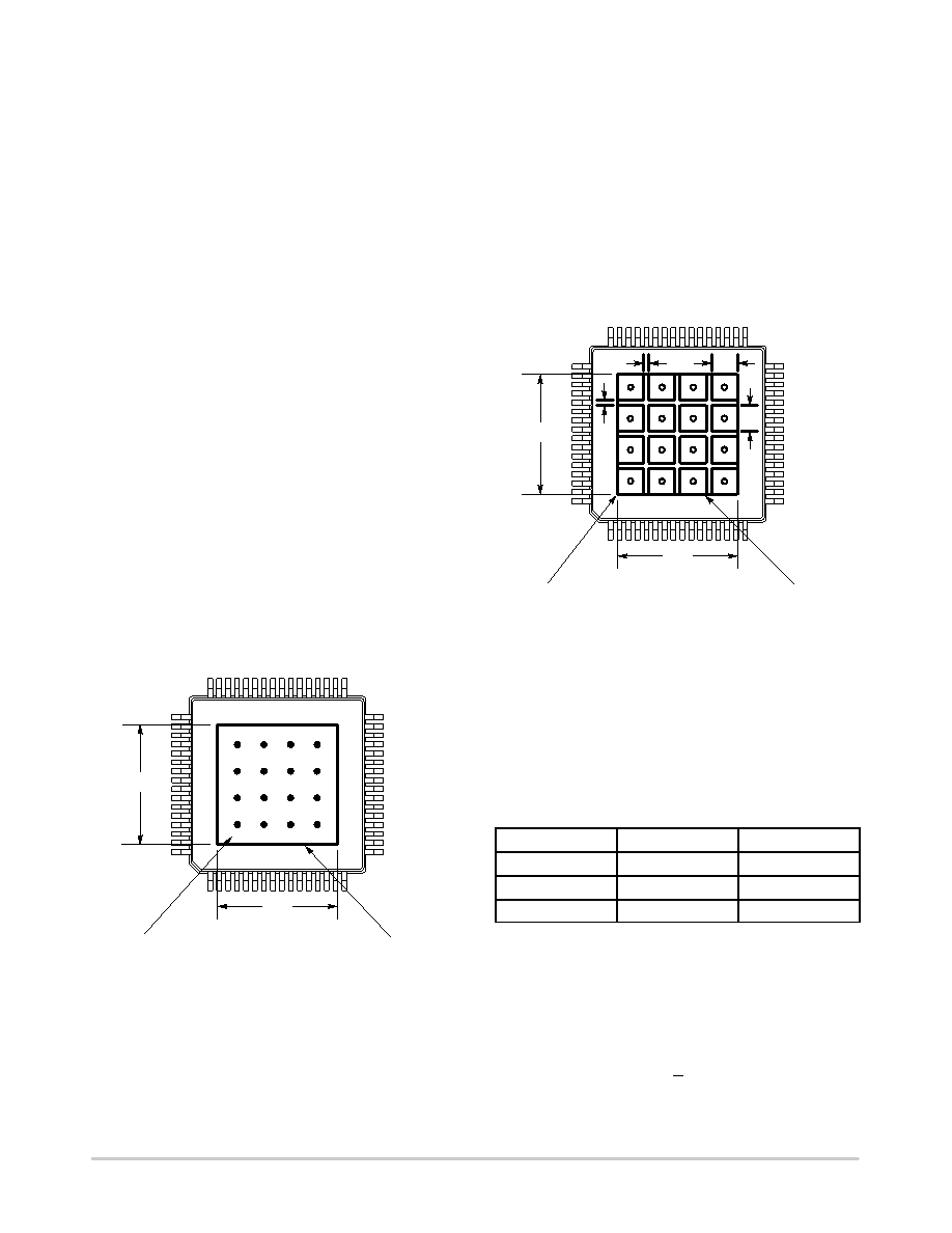
The recommended thermal land design for NB100EP223
applications on multilayer boards comprises a 4 X 4
thermal via array using a 1.2 mm pitch as shown in Figure 8
providing an efficient heat removal path.
Figure 8. Recommended Thermal Land Pattern
All Units mm
Thermal Via Array (4 X 4)
1.2 mm Pitch
0.3 mm Diameter
Exposed Pad
Land Pattern
4.6
The via diameter should be approximately 0.3 mm with
1 oz. copper via barrel plating. Solder wicking inside the via
may result in voiding during the solder process and must be
avoided. If the copper plating does not plug the vias, stencil
print solder paste onto the printed circuit pad. This will
supply enough solder paste to fill those vias and not starve
the solder joints. The attachment process for the exposed pad
package is equivalent to standard surface mount packages.
Figure 9, “Recommended solder mask openings”, shows a
recommended solder mask opening with respect to a 4 X 4
thermal via array. Because a large solder mask opening may
result in a poor rework release, the opening should be
subdivided as shown in Figure 9. For the nominal package
standoff of 0.1 mm, a stencil thickness of 5 to 8 mils should
be considered.
Figure 9. Recommended Solder Mask Openings
All Units mm
Thermal Via Array (4 X 4)
1.2 mm Pitch
0.3 mm Diameter
Exposed Pad
Land Pattern
4.6
0.2
1.0
0.2
Proper thermal management is critical for reliable system
operation. This is especially true for highfanout and high
output drive capability products.
For thermal system analysis and junction temperature
calculation the thermal resistance parameters of the package
is provided:
Table 9. Thermal Resistance *
lfpm
qJA 5C/W
qJC 5C/W
0
35.6
3.2
100
32.8
4.9
500
30.0
6.4
* Junction to ambient and Junction to board, fourconductor
layer test board (2S2P) per JESD 518
These recommendations are to be used as a guideline,
only. It is therefore recommended that users employ
sufficient thermal modeling analysis to assist in applying the
general recommendations to their particular application to
assure adequate thermal performance. The exposed pad of
the NB100EP223 package is electrically shorted to the
substrate of the integrated circuit and GND. The thermal
land should be electrically connected to GND.
相关PDF资料 |
PDF描述 |
|---|---|
| V300A36H500BF2 | CONVERTER MOD DC/DC 36V 500W |
| SY100E111LEJC TR | IC CLK FANOUT BUFFER 1:9 28-PLCC |
| AD9760ARZ50RL | IC DAC 10BIT 125MSPS 28TSSOP |
| V300A36H500BF | CONVERTER MOD DC/DC 36V 500W |
| SY100E111LEJC | IC CLK FANOUT BUFFER 1:9 28-PLCC |
相关代理商/技术参数 |
参数描述 |
|---|---|
| NB100LVEP17 | 制造商:ONSEMI 制造商全称:ON Semiconductor 功能描述:2.5V / 3.3V Quad Differential Driver/Receiver |
| NB100LVEP17/D | 制造商:未知厂家 制造商全称:未知厂家 功能描述:2.5V / 3.3V ECL Quad Differential Driver/Receiver |
| NB100LVEP17DT | 功能描述:总线接收器 2.5V/3.3V/5V ECL RoHS:否 制造商:Texas Instruments 接收机数量:4 接收机信号类型:Differential 接口类型:EIA/TIA-422-B, V.11 工作电源电压:3.3 V 最大工作温度:+ 85 C 最小工作温度:- 40 C 封装 / 箱体:TSSOP-16 封装:Reel |
| NB100LVEP17DTG | 功能描述:总线接收器 2.5V/3.3V/5V ECL Quad Diff Driver RoHS:否 制造商:Texas Instruments 接收机数量:4 接收机信号类型:Differential 接口类型:EIA/TIA-422-B, V.11 工作电源电压:3.3 V 最大工作温度:+ 85 C 最小工作温度:- 40 C 封装 / 箱体:TSSOP-16 封装:Reel |
| NB100LVEP17DTR2 | 功能描述:总线接收器 2.5V/3.3V/5V ECL RoHS:否 制造商:Texas Instruments 接收机数量:4 接收机信号类型:Differential 接口类型:EIA/TIA-422-B, V.11 工作电源电压:3.3 V 最大工作温度:+ 85 C 最小工作温度:- 40 C 封装 / 箱体:TSSOP-16 封装:Reel |
发布紧急采购,3分钟左右您将得到回复。