- 您现在的位置:买卖IC网 > PDF目录8676 > NB100EP223FAR2G (ON Semiconductor)IC CLOCK BUFFER MUX 2:22 64-LQFP PDF资料下载
参数资料
| 型号: | NB100EP223FAR2G |
| 厂商: | ON Semiconductor |
| 文件页数: | 5/10页 |
| 文件大小: | 0K |
| 描述: | IC CLOCK BUFFER MUX 2:22 64-LQFP |
| 标准包装: | 1,500 |
| 系列: | 100EP |
| 类型: | 扇出缓冲器(分配),多路复用器 |
| 电路数: | 1 |
| 比率 - 输入:输出: | 2:22 |
| 差分 - 输入:输出: | 是/是 |
| 输入: | HSTL,LVDS,LVPECL |
| 输出: | HSTL |
| 频率 - 最大: | 500MHz |
| 电源电压: | 3 V ~ 3.6 V |
| 工作温度: | 0°C ~ 85°C |
| 安装类型: | 表面贴装 |
| 封装/外壳: | 64-LQFP 裸露焊盘 |
| 供应商设备封装: | 64-LQFP(10x10) |
| 包装: | 带卷 (TR) |
| 其它名称: | NB100EP223FAR2GOS |
NB100EP223
http://onsemi.com
4
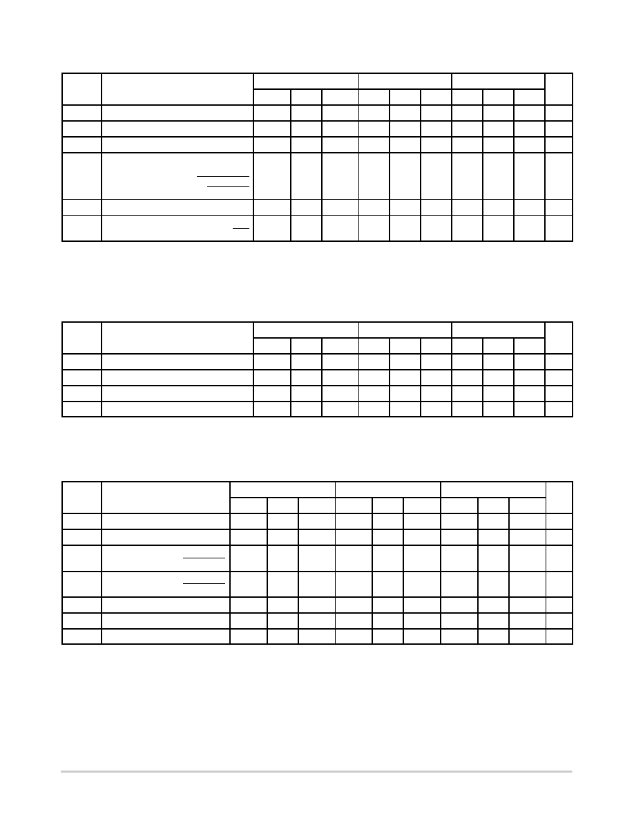
Table 5. LVPECL DC CHARACTERISTICS VCC = 3.3 V; VCCO = 1.8 V; GND = 0 V
Symbol
Characteristic
0°C
25°C
85°C
Unit
Min
Typ
Max
Min
Typ
Max
Min
Typ
Max
ICC
Power Supply Current
VCC
82
100
130
82
100
130
82
100
130
mA
VIH
Input HIGH Voltage (SingleEnded)
2135
2420
2135
2420
2135
2420
mV
VIL
Input LOW Voltage (SingleEnded)
1490
1675
1490
1675
1490
1675
mV
VIHCMR
Input HIGH Voltage Common Mode
LVPECL_CLK/LVPECL_CLK
HSTL_CLK/HSTL_CLK
1.2
0.3
3.3
1.6
1.2
0.3
3.3
1.6
1.2
0.3
3.3
1.6
V
IIH
Input HIGH Current
150
mA
IIL
Input LOW Current
CLK
0.5
150
0.5
150
0.5
150
mA
NOTE: Device will meet the specifications after thermal equilibrium has been established when mounted in a test socket or printed circuit
board with maintained transverse airflow greater than 500 lfpm. Electrical parameters are guaranteed only over the declared
operating temperature range. Functional operation of the device exceeding these conditions is not implied. Device specification limit
values are applied individually under normal operating conditions and not valid simultaneously.
2. VIHCMR min varies 1:1 with VCC. The VIHCMR range is referenced to the most positive side of the differential input signal.
Table 6. LVTTL/LVCMOS DC CHARACTERISTICS VCC = 3.3 V; VCCO = 1.8 V; GND = 0 V
Symbol
Characteristic
0°C
25°C
85°C
Unit
Min
Typ
Max
Min
Typ
Max
Min
Typ
Max
VIH
Input HIGH Voltage
2.0
V
VIL
Input LOW Voltage
0.8
V
IIH
Input HIGH Current
150
mA
IIL
Input LOW Current
300
mA
NOTE: Device will meet the specifications after thermal equilibrium has been established when mounted in a test socket or printed circuit
board with maintained transverse airflow greater than 500 lfpm. Electrical parameters are guaranteed only over the declared
operating temperature range. Functional operation of the device exceeding these conditions is not implied. Device specification limit
values are applied individually under normal operating conditions and not valid simultaneously.
Table 7. HSTL DC CHARACTERISTICS VCC = 3.3 V; VCCO = 1.62.0 V; GND = 0 V
Symbol
Characteristic
0°C
25°C
85°C
Unit
Min
Typ
Max
Min
Typ
Max
Min
Typ
Max
VOH
Output HIGH Voltage (Note 3)
1000
1200
1000
1200
1000
1200
mV
VOL
Output LOW Voltage (Note 3)
0
400
0
400
0
400
mV
VIH
Input HIGH Voltage (Differential)
HSTL_CLK/HSTL_CLK VX+100
1600
VX+100
1600
VX+100
1600
mV
VIL
Input LOW Voltage (Differential)
HSTL_CLK/HSTL_CLK
300
VX100
300
VX100
300
VX100 mV
VX
Differential Cross Point Voltage
680
900
680
900
680
900
mV
IIH
Input HIGH Current
150
mA
IIL
Input LOW Current
300
mA
NOTE: Device will meet the specifications after thermal equilibrium has been established when mounted in a test socket or printed circuit
board with maintained transverse airflow greater than 500 lfpm. Electrical parameters are guaranteed only over the declared
operating temperature range. Functional operation of the device exceeding these conditions is not implied. Device specification limit
values are applied individually under normal operating conditions and not valid simultaneously.
3. All outputs loaded with 50 W to GND (See Figure 6).
相关PDF资料 |
PDF描述 |
|---|---|
| V300A36H500BF2 | CONVERTER MOD DC/DC 36V 500W |
| SY100E111LEJC TR | IC CLK FANOUT BUFFER 1:9 28-PLCC |
| AD9760ARZ50RL | IC DAC 10BIT 125MSPS 28TSSOP |
| V300A36H500BF | CONVERTER MOD DC/DC 36V 500W |
| SY100E111LEJC | IC CLK FANOUT BUFFER 1:9 28-PLCC |
相关代理商/技术参数 |
参数描述 |
|---|---|
| NB100LVEP17 | 制造商:ONSEMI 制造商全称:ON Semiconductor 功能描述:2.5V / 3.3V Quad Differential Driver/Receiver |
| NB100LVEP17/D | 制造商:未知厂家 制造商全称:未知厂家 功能描述:2.5V / 3.3V ECL Quad Differential Driver/Receiver |
| NB100LVEP17DT | 功能描述:总线接收器 2.5V/3.3V/5V ECL RoHS:否 制造商:Texas Instruments 接收机数量:4 接收机信号类型:Differential 接口类型:EIA/TIA-422-B, V.11 工作电源电压:3.3 V 最大工作温度:+ 85 C 最小工作温度:- 40 C 封装 / 箱体:TSSOP-16 封装:Reel |
| NB100LVEP17DTG | 功能描述:总线接收器 2.5V/3.3V/5V ECL Quad Diff Driver RoHS:否 制造商:Texas Instruments 接收机数量:4 接收机信号类型:Differential 接口类型:EIA/TIA-422-B, V.11 工作电源电压:3.3 V 最大工作温度:+ 85 C 最小工作温度:- 40 C 封装 / 箱体:TSSOP-16 封装:Reel |
| NB100LVEP17DTR2 | 功能描述:总线接收器 2.5V/3.3V/5V ECL RoHS:否 制造商:Texas Instruments 接收机数量:4 接收机信号类型:Differential 接口类型:EIA/TIA-422-B, V.11 工作电源电压:3.3 V 最大工作温度:+ 85 C 最小工作温度:- 40 C 封装 / 箱体:TSSOP-16 封装:Reel |
发布紧急采购,3分钟左右您将得到回复。