参数资料
| 型号: | NB3N3002DTR2G |
| 厂商: | ON Semiconductor |
| 文件页数: | 3/8页 |
| 文件大小: | 0K |
| 描述: | IC CLK GEN XTAL-HCSL 16-TSSOP |
| 标准包装: | 2,500 |
| 类型: | 时钟发生器 |
| PLL: | 是 |
| 输入: | 晶体 |
| 输出: | HCSL |
| 电路数: | 1 |
| 比率 - 输入:输出: | 1:1 |
| 差分 - 输入:输出: | 无/是 |
| 频率 - 最大: | 200MHz |
| 除法器/乘法器: | 是/无 |
| 电源电压: | 3.135 V ~ 3.465 V |
| 工作温度: | -40°C ~ 85°C |
| 安装类型: | 表面贴装 |
| 封装/外壳: | 16-TSSOP(0.173",4.40mm 宽) |
| 供应商设备封装: | 16-TSSOP |
| 包装: | 带卷 (TR) |
NB3N3002
http://onsemi.com
3
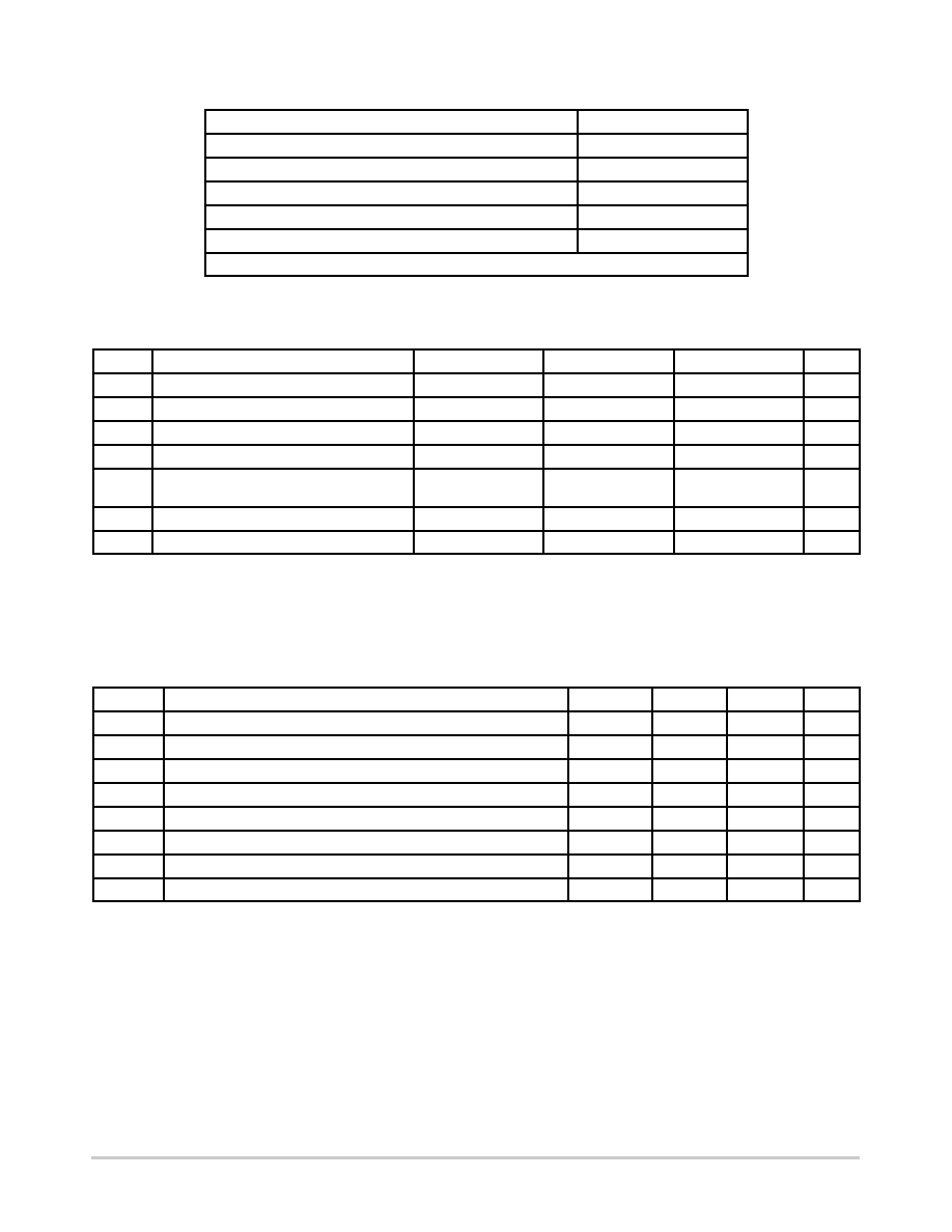
Table 3. ATTRIBUTES
Characteristic
Value
ESD Protection
Human Body Model
> 2 kV
RPU OE, SEL0 and SEL1 Pullup Resistor
100 kW
Moisture Sensitivity, Indefinite Time Out of Dry Pack (Note 1)
Level 1
Flammability Rating
Oxygen Index: 28 to 34
UL 94 V0 @ 0.125 in
Transistor Count
7623
Meets or exceeds JEDEC Spec EIA/JESD78 IC Latchup Test
1. For additional information, see Application Note AND8003/D.
Table 4. MAXIMUM RATINGS (Note 2)
Symbol
Parameter
Condition 1
Condition 2
Rating
Units
VDD
Positive Power Supply
GND = 0 V
4.6
V
VI
Input Voltage (VIN)
GND = 0 V
GND v VI v VDD
0.5 V to VDD+0.5 V
V
TA
Operating Temperature Range
40 to +85
°C
Tstg
Storage Temperature Range
65 to +150
°C
qJA
Thermal Resistance (JunctiontoAmbient)
0 lfpm
500 lfpm
TSSOP–16
138
108
°C/W
qJC
Thermal Resistance (JunctiontoCase)
(Note 3)
TSSOP16
33 to 36
°C/W
Tsol
Wave Solder
265
°C
Stresses exceeding Maximum Ratings may damage the device. Maximum Ratings are stress ratings only. Functional operation above the
Recommended Operating Conditions is not implied. Extended exposure to stresses above the Recommended Operating Conditions may affect
device reliability.
2. Maximum ratings applied to the device are individual stress limit values (not normal operating conditions) and not valid simultaneously. If
stress limits are exceeded device functional operation is not implied, damage may occur and reliability may be affected.
3. JEDEC standard multilayer board 2S2P (2 signal, 2 power).
Table 5. DC CHARACTERISTICS (VDD = 3.3 V ±5%, GND = 0 V, TA = 40°C to +85°C)
Symbol
Characteristic
Min
Typ
Max
Unit
IDD
Power Supply Current (Note 4)
65
95
mA
IDDOE
Power Supply Current when OE is Set Low
35
65
mA
VIH
Input HIGH Voltage (X1/CLK, Sel0, Sel1,and OE)
0.7 * VDD
VDD + 300
mV
VIL
Input LOW Voltage (X1/CLK, Sel0, Sel1, and OE)
GND 300
0.3* VDD
mV
VOH
Output HIGH Voltage (See Figure 4)
660
700
850
mV
VOL
Output LOW Voltage (See Figure 4)
150
0
150
mV
Vcross
Crossing Voltage Magnitude (Absolute)
250
400
mV
DVcross
Change in Magnitude of Vcross
150
mV
NOTE: Device will meet the specifications after thermal equilibrium has been established when mounted in a test socket or printed circuit
board with maintained transverse airflow greater than 500 lfpm. Electrical parameters are guaranteed only over the declared
operating temperature range. Functional operation of the device exceeding these conditions is not implied. Device specification limit
values are applied individually under normal operating conditions and not valid simultaneously.
4. NB3N circuits are designed to meet the DC specifications shown in the above table after thermal equilibrium has been established. The circuit
is in a test socket or mounted on a printed circuit board and transverse airflow greater than 500 lfpm is maintained.
5. Measurement taken with outputs terminated with RS = 33.2 W, RL = 49.9 W, with load capacitance of 2 pF and current biasing resistor, RREF,
相关PDF资料 |
PDF描述 |
|---|---|
| VE-BVV-MY-F2 | CONVERTER MOD DC/DC 5.8V 50W |
| VE-B6V-MV-F4 | CONVERTER MOD DC/DC 5.8V 150W |
| VE-2VY-MX-F1 | CONVERTER MOD DC/DC 3.3V 49.5W |
| MAX13055EEWG+T | IC TRANSLATOR LL 8CH 24WLP |
| MAX13030EEBE+T | IC TRANSLATOR LL 6CH 16UCSP |
相关代理商/技术参数 |
参数描述 |
|---|---|
| NB3N3010BDG | 功能描述:时钟发生器及支持产品 AUDIO OVERSAMPLING RoHS:否 制造商:Silicon Labs 类型:Clock Generators 最大输入频率:14.318 MHz 最大输出频率:166 MHz 输出端数量:16 占空比 - 最大:55 % 工作电源电压:3.3 V 工作电源电流:1 mA 最大工作温度:+ 85 C 安装风格:SMD/SMT 封装 / 箱体:QFN-56 |
| NB3N3010BDR2G | 功能描述:时钟发生器及支持产品 AUDIO OVERSAMPLING CLOCK RoHS:否 制造商:Silicon Labs 类型:Clock Generators 最大输入频率:14.318 MHz 最大输出频率:166 MHz 输出端数量:16 占空比 - 最大:55 % 工作电源电压:3.3 V 工作电源电流:1 mA 最大工作温度:+ 85 C 安装风格:SMD/SMT 封装 / 箱体:QFN-56 |
| NB3N3011 | 制造商:ONSEMI 制造商全称:ON Semiconductor 功能描述:3.3 V 100 MHz / 106.25 MHz PureEdge Clock Generator with LVPECL Differential Output |
| NB3N3011DTEVB | 功能描述:BOARD EVAL FOR NB3N3011 RoHS:是 类别:编程器,开发系统 >> 评估演示板和套件 系列:* 标准包装:1 系列:PCI Express® (PCIe) 主要目的:接口,收发器,PCI Express 嵌入式:- 已用 IC / 零件:DS80PCI800 主要属性:- 次要属性:- 已供物品:板 |
| NB3N3011DTG | 功能描述:时钟合成器/抖动清除器 XTAL 3.3V LVPECL CLK RoHS:否 制造商:Skyworks Solutions, Inc. 输出端数量: 输出电平: 最大输出频率: 输入电平: 最大输入频率:6.1 GHz 电源电压-最大:3.3 V 电源电压-最小:2.7 V 封装 / 箱体:TSSOP-28 封装:Reel |
发布紧急采购,3分钟左右您将得到回复。