参数资料
| 型号: | NB6L11SMNG |
| 厂商: | ON Semiconductor |
| 文件页数: | 1/11页 |
| 文件大小: | 0K |
| 描述: | IC CLK BUFFER TRANSLA 1:2 16-QFN |
| 标准包装: | 123 |
| 系列: | AnyLevel™ |
| 类型: | 扇出缓冲器(分配),变换器 |
| 电路数: | 1 |
| 比率 - 输入:输出: | 1:2 |
| 差分 - 输入:输出: | 是/是 |
| 输入: | CML,LVCMOS,LVDS,LVPECL,LVTTL |
| 输出: | LVDS |
| 频率 - 最大: | 2GHz |
| 电源电压: | 2.375 V ~ 3.63 V |
| 工作温度: | -40°C ~ 85°C |
| 安装类型: | 表面贴装 |
| 封装/外壳: | 16-VFQFN 裸露焊盘 |
| 供应商设备封装: | 16-QFN(3x3) |
| 包装: | 管件 |
| 产品目录页面: | 1115 (CN2011-ZH PDF) |
| 其它名称: | NB6L11SMNG-ND NB6L11SMNGOS |
Semiconductor Components Industries, LLC, 2009
August, 2009 Rev. 7
1
Publication Order Number:
NB6L11S/D
NB6L11S
2.5 V 1:2 AnyLevel] Input
to LVDS Fanout Buffer /
Translator
The NB6L11S is a differential 1:2 clock or data receiver and will
accept AnyLevel
input signals: LVPECL, CML, LVCMOS, LVTTL,
or LVDS. These signals will be translated to LVDS and two identical
copies of Clock or Data will be distributed, operating up to 2.0 GHz or
2.5 Gb/s, respectively. As such, the NB6L11S is ideal for SONET,
GigE, Fiber Channel, Backplane and other Clock or Data distribution
applications.
The NB6L11S has a wide input common mode range from
GND + 50 mV to VCC 50 mV. Combined with the 50 W internal
termination resistors at the inputs, the NB6L11S is ideal for translating
a variety of differential or singleended Clock or Data signals to
350 mV typical LVDS output levels.
The NB6L11S is the 2.5 V version of the NB6N11S and is offered in
a small 3 mm X 3 mm 16QFN package. Application notes, models,
and support documentation are available at www.onsemi.com.
Features
Input Clock Frequency > 2.0 GHz
Input Data Rate > 2.5 Gb/s
RMS Clock Jitter 0.5 ps, Typical
622 Mb/s Data Dependent Jitter 6 ps, Typical
380 ps Typical Propagation Delay
120 ps Typical Rise and Fall Times
Single Power Supply; VCC = 2.5 V " 5%
These are PbFree Devices
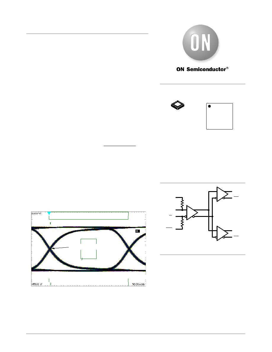
TIME (58 ps/div)
Figure 2. Typical Output Waveform at 2.488 Gb/s with
PRBS 2231 (VINPP = 400 mV; Input Signal DDJ = 14 ps)
VOL
TAGE
(130
mV/div)
Device DDJ = 10 ps
A
= Assembly Location
L
= Wafer Lot
Y
= Year
W
= Work Week
G
= PbFree Package
*For additional marking information, refer to
Application Note AND8002/D.
MARKING
DIAGRAM*
QFN16
MN SUFFIX
CASE 485G
http://onsemi.com
See detailed ordering and shipping information in the package
dimensions section on page 10 of this data sheet.
ORDERING INFORMATION
16
NB6L
11S
ALYW G
G
1
1
Q0
Q1
D
VTD
Figure 1. Logic Diagram
(Note: Microdot may be in either location)
相关PDF资料 |
PDF描述 |
|---|---|
| LTC2621CDD-1#PBF | IC DAC 12BIT R-R 10-DFN |
| VE-JNW-MZ-F2 | CONVERTER MOD DC/DC 5.5V 25W |
| VE-JNV-MZ-F4 | CONVERTER MOD DC/DC 5.8V 25W |
| LTC2621CDD | IC DAC 12BIT SGL R-R VOUT 10DFN |
| AD5425YRM-REEL7 | IC DAC 8BIT MULTIPLYING 10-MSOP |
相关代理商/技术参数 |
参数描述 |
|---|---|
| NB6L11SMNGEVB | 功能描述:BOARD EVAL FOR NB6L11SMNG RoHS:是 类别:编程器,开发系统 >> 评估演示板和套件 系列:- 标准包装:1 系列:PCI Express® (PCIe) 主要目的:接口,收发器,PCI Express 嵌入式:- 已用 IC / 零件:DS80PCI800 主要属性:- 次要属性:- 已供物品:板 |
| NB6L11SMNR2G | 功能描述:时钟缓冲器 HF LVDS FANOUT BUFF/ TRANS RoHS:否 制造商:Texas Instruments 输出端数量:5 最大输入频率:40 MHz 传播延迟(最大值): 电源电压-最大:3.45 V 电源电压-最小:2.375 V 最大功率耗散: 最大工作温度:+ 85 C 最小工作温度:- 40 C 封装 / 箱体:LLP-24 封装:Reel |
| NB6L14 | 制造商:ONSEMI 制造商全称:ON Semiconductor 功能描述:2.5 V/3.3 V 3.0 GHz Differential 1:4 LVPECL Fanout Buffer |
| NB6L14_07 | 制造商:ONSEMI 制造商全称:ON Semiconductor 功能描述:2.5 V/3.3 V 3.0 GHz Differential 1:4 LVPECL Fanout Buffer |
| NB6L14M | 制造商:ONSEMI 制造商全称:ON Semiconductor 功能描述:2.5 V/3.3 V 3.0 GHz Differential 1:4 CML Fanout Buffer |
发布紧急采购,3分钟左右您将得到回复。