参数资料
| 型号: | NB6L11SMNG |
| 厂商: | ON Semiconductor |
| 文件页数: | 7/11页 |
| 文件大小: | 0K |
| 描述: | IC CLK BUFFER TRANSLA 1:2 16-QFN |
| 标准包装: | 123 |
| 系列: | AnyLevel™ |
| 类型: | 扇出缓冲器(分配),变换器 |
| 电路数: | 1 |
| 比率 - 输入:输出: | 1:2 |
| 差分 - 输入:输出: | 是/是 |
| 输入: | CML,LVCMOS,LVDS,LVPECL,LVTTL |
| 输出: | LVDS |
| 频率 - 最大: | 2GHz |
| 电源电压: | 2.375 V ~ 3.63 V |
| 工作温度: | -40°C ~ 85°C |
| 安装类型: | 表面贴装 |
| 封装/外壳: | 16-VFQFN 裸露焊盘 |
| 供应商设备封装: | 16-QFN(3x3) |
| 包装: | 管件 |
| 产品目录页面: | 1115 (CN2011-ZH PDF) |
| 其它名称: | NB6L11SMNG-ND NB6L11SMNGOS |
NB6L11S
http://onsemi.com
5
Symbol
Characteristic
40°C
25°C
85°C
Unit
Min
Typ
Max
Min
Typ
Max
Min
Typ
Max
VOUTPP Output Voltage Amplitude (@ VINPPmin)fin ≤ 1.0 GHz
(Figure 4)
fin= 1.5 GHz
fin= 2.0 GHz
220
200
170
350
300
270
220
200
170
350
300
270
220
200
170
350
300
270
mV
fDATA
Maximum Operating Data Rate
1.5
2.5
1.5
2.5
1.5
2.5
Gb/s
tPLH,
tPHL
Differential Input to Differential Output
Propagation Delay
250
450
250
380
450
250
450
ps
tSKEW
Duty Cycle Skew (Note 11)
Within Device Skew (Note 16)
DevicetoDevice Skew (Note 15)
8
5
30
45
25
100
8
5
30
45
25
100
8
5
30
45
25
100
ps
tJITTER
RMS Random Clock Jitter (Note 13)
fin = 1.0 GHz
fin = 1.5 GHz
PeaktoPeak Data Dependent Jitter (Note 14)
fDATA = 622 Mb/s
fDATA = 1.5 Gb/s
fDATA = 2.488 Gb/s
0.5
6
7
10
0.5
6
7
10
0.5
6
7
10
ps
VINPP
Input Voltage Swing/Sensitivity
(Differential Configuration) (Note 12)
100
VCC
GND
100
VCC
GND
100
VCC
GND
mV
tr
tf
Output Rise/Fall Times @ 250 MHz
Q, Q
(20% 80%)
70
120
170
70
120
170
70
120
170
ps
NOTE: Device will meet the specifications after thermal equilibrium has been established when mounted in a test socket or printed circuit
board with maintained transverse airflow greater than 500 lfpm. Electrical parameters are guaranteed only over the declared
operating temperature range. Functional operation of the device exceeding these conditions is not implied. Device specification limit
values are applied individually under normal operating conditions and not valid simultaneously.
10.Measured by forcing VINPPmin with 50% duty cycle clock source and VCC 1400 mV offset. All loading with an external RL = 100 W across
“D” and “D” of the receiver. Input edge rates 150 ps (20%80%).
11. See Figure 17 differential measurement of tskew = |tPLH tPHL| for a nominal 50% differential clock input waveform @ 250 MHz.
12.Input voltage swing is a singleended measurement operating in differential mode.
13.RMS jitter with 50% Duty Cycle input clock signal.
14.Deterministic jitter with input NRZ data at PRBS 2231 and K28.5.
15.Skew is measured between outputs under identical transition @ 250 MHz.
16.The worst case condition between Q0/Q0 and Q1/Q1 from either D0/D0 or D1/D1, when both outputs have the same transition.
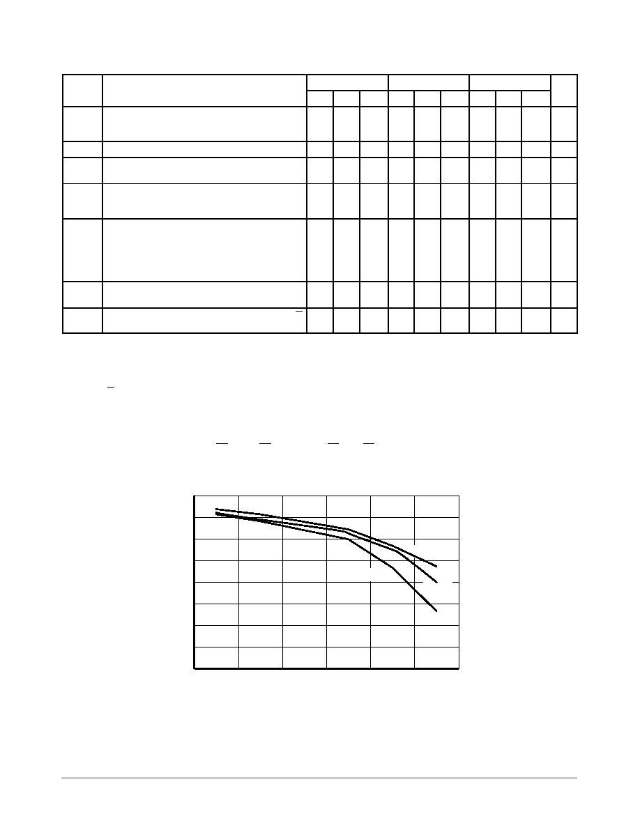
INPUT CLOCK FREQUENCY (GHz)
Figure 4. Output Voltage Amplitude (VOUTPP) versus
Input Clock Frequency (fin) and Temperature (@ VCC = 2.5 V)
OUTPUT
VOL
TAGE
AMPLITUDE
(mV)
0
50
100
150
200
250
300
350
400
0.5
1
1.5
2
2.5
3
0
85°C
40°C
25°C
相关PDF资料 |
PDF描述 |
|---|---|
| LTC2621CDD-1#PBF | IC DAC 12BIT R-R 10-DFN |
| VE-JNW-MZ-F2 | CONVERTER MOD DC/DC 5.5V 25W |
| VE-JNV-MZ-F4 | CONVERTER MOD DC/DC 5.8V 25W |
| LTC2621CDD | IC DAC 12BIT SGL R-R VOUT 10DFN |
| AD5425YRM-REEL7 | IC DAC 8BIT MULTIPLYING 10-MSOP |
相关代理商/技术参数 |
参数描述 |
|---|---|
| NB6L11SMNGEVB | 功能描述:BOARD EVAL FOR NB6L11SMNG RoHS:是 类别:编程器,开发系统 >> 评估演示板和套件 系列:- 标准包装:1 系列:PCI Express® (PCIe) 主要目的:接口,收发器,PCI Express 嵌入式:- 已用 IC / 零件:DS80PCI800 主要属性:- 次要属性:- 已供物品:板 |
| NB6L11SMNR2G | 功能描述:时钟缓冲器 HF LVDS FANOUT BUFF/ TRANS RoHS:否 制造商:Texas Instruments 输出端数量:5 最大输入频率:40 MHz 传播延迟(最大值): 电源电压-最大:3.45 V 电源电压-最小:2.375 V 最大功率耗散: 最大工作温度:+ 85 C 最小工作温度:- 40 C 封装 / 箱体:LLP-24 封装:Reel |
| NB6L14 | 制造商:ONSEMI 制造商全称:ON Semiconductor 功能描述:2.5 V/3.3 V 3.0 GHz Differential 1:4 LVPECL Fanout Buffer |
| NB6L14_07 | 制造商:ONSEMI 制造商全称:ON Semiconductor 功能描述:2.5 V/3.3 V 3.0 GHz Differential 1:4 LVPECL Fanout Buffer |
| NB6L14M | 制造商:ONSEMI 制造商全称:ON Semiconductor 功能描述:2.5 V/3.3 V 3.0 GHz Differential 1:4 CML Fanout Buffer |
发布紧急采购,3分钟左右您将得到回复。