- 您现在的位置:买卖IC网 > PDF目录19365 > IR2521DSTRPBF (International Rectifier)IC BALLAST CTLR ADAPTIVE 8-SOIC PDF资料下载
参数资料
| 型号: | IR2521DSTRPBF |
| 厂商: | International Rectifier |
| 文件页数: | 9/17页 |
| 文件大小: | 0K |
| 描述: | IC BALLAST CTLR ADAPTIVE 8-SOIC |
| 标准包装: | 1 |
| 封装/外壳: | 8-SOIC(0.154",3.90mm 宽) |
| 供应商设备封装: | 8-SOIC |
| 包装: | 标准包装 |
| 其它名称: | IR2521DSTRPBFDKR |
�� �
�
�IR2520D(S)� &� (PbF)�
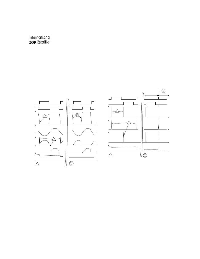
�lamp� removal� (open� circuit),� a� dropping� DC� bus� during� a�
�mains� brown-out� or� mains� interrupt,� lamp� variations� over�
�time,� or� component� variations.� To� protect� against� this,� an�
�internal� high-voltage� MOSFET� is� turned� on� at� the� turn-off� of�
�HO� and� the� VS-sensing� circuit� measures� VS� at� each� rising�
�edge� of� LO.� If� the� VS� voltage� is� non-zero,� a� pulse� of� current�
�is� sinked� from� the� VCO� pin� (Figures� 5� and� 6)� to� slightly�
�discharge� the� external� capacitor,� CVCO,� causing� the�
�frequency� to� increase� slightly.� The� VCO� capacitor� then�
�charges� up� during� the� rest� of� the� cycle� slowly� due� to� the�
�open� circuit� (Figure� 7).� This� will� cause� capacitive� switching�
�(hard-switching)� resulting� in� high� peak� MOSFET� currents�
�that� can� damage� them.� The� IR2520D� will� increase� the� fre-�
�quency� in� attempt� to� satisfy� ZVS� until� the� VCO� pin� de-�
�creases� below� 0.82V� (V� VCOSD� ).� The� IC� will� enter� Fault�
�Mode� and� latch� the� LO� and� HO� gate� driver� outputs� ‘low’� for�
�turning� the� half-bridge� off� safely� before� any� damage� can�
�occur� to� the� MOSFETs.�
�internal� current� source.�
�V� LO�
�V� HO�
�!�
�V� VS�
�V� LO�
�V� HO�
�V� VS�
�IMLS�
�!�
�!�
�RUN� MODE�
�FAULT MOD� E�
�IL�
�IMHS�
�IMLS�
�!�
�IMHS�
�VVCO�
�0.85V�
�VVCO�
�!�
�Capacitive� switching.� Hard-switching�
�and� high� peak� MOSFET� currents!�
�Frequency� shifted� higher�
�until� VCO� <� 0.82V.� LO� and�
�HO� are� latched� low� before�
�damage� occurs� to� MOSFETs.�
�!�
�Too� close� to� resonance.�
�Hard-switching� and� high�
�peak� MOSFET� currents!�
�Frequency� shifted� higher�
�to� maintain� ZVS.�
�Fig.� 7� Lamp� removal� or� open� filament� fault�
�condition� timing� diagram�
�Fig.� 6� IR2520D� non-ZVS� protection� timing� diagram.�
�The� frequency� is� trying� to� decrease� towards� resonance�
�by� charging� the� VCO� capacitor� and� the� adaptive� ZVS� cir-�
�cuit� “nudges”� the� frequency� back� up� slightly� above� reso-�
�nance� each� time� non-ZVS� is� detected� at� the� turn-on� of� LO.�
�The� internal� high-voltage� MOSFET� is� then� turned� off� at� the�
�turn-off� of� LO� and� it� withstands� the� high-voltage� when� VS�
�slews� up� to� the� DC� bus� potential.� The� circuit� then� remains� in�
�this� closed-loop� adaptive� ZVS� mode� during� running� and�
�maintains� ZVS� operation� with� changing� line� conditions,� com-�
�ponent� tolerance� variations� and� lamp/load� variations.� Dur-�
�ing� a� lamp� removal� or� filament� failure,� the� lamp� resonant�
�tank� will� be� interrupted� causing� the� half-bridge� output� to� go�
�www.irf.com�
�Crest� Factor� Over-current� Protection�
�During� normal� lamp� ignition,� the� frequency� sweeps� through�
�resonance� and� the� output� voltage� increases� across� the�
�resonant� capacitor� and� lamp� until� the� lamp� ignites.� If� the�
�lamp� fails� to� ignite,� the� resonant� capacitor� voltage,� the� inductor�
�voltage� and� inductor� current� will� continue� to� increase� until�
�the� inductor� saturates� or� the� output� voltage� exceeds� the�
�maximum� voltage� rating� of� the� resonant� capacitor� or� inductor.�
�The� ballast� must� shutdown� before� damage� occurs.� To�
�protect� against� a� lamp� non-strike� fault� condition,� the� IR2520D�
�uses� the� VS-sensing� circuitry� (Figure� 5)� to� also� measure�
�the� low-side� half-bridge� MOSFET� current� for� detecting� an�
�9�
�相关PDF资料 |
PDF描述 |
|---|---|
| S392K59Y5PP63K7R | CAP CER 3900PF 2KV 10% RADIAL |
| 5-787355-1 | CONN RCPT 9POS VERT SOLDER CUP |
| ECC08DRTF-S13 | CONN EDGECARD 16POS .100 EXTEND |
| 1N5406RLG | DIODE STD REC 3A 600V DO201AD |
| S332K53Y5PP63K7R | CAP CER 3300PF 2KV 10% RADIAL |
相关代理商/技术参数 |
参数描述 |
|---|---|
| NB6L295MNG | 功能描述:延迟线/计时元素 LVPECL DUAL PRG DLAY RoHS:否 制造商:Micrel 功能:Active Programmable Delay Line 传播延迟时间:1000 ps 工作温度范围: 封装 / 箱体:QFN-24 封装:Tube |
| NB6L295MNGEVB | 功能描述:电源管理IC开发工具 NB6L295 EVAL BOARD RoHS:否 制造商:Maxim Integrated 产品:Evaluation Kits 类型:Battery Management 工具用于评估:MAX17710GB 输入电压: 输出电压:1.8 V |
| NB6L295MNTXG | 功能描述:延迟线/计时元素 LVPECL DUAL PRG DLAY RoHS:否 制造商:Micrel 功能:Active Programmable Delay Line 传播延迟时间:1000 ps 工作温度范围: 封装 / 箱体:QFN-24 封装:Tube |
| NB6L56MNG | 功能描述:时钟缓冲器 TSMC 2.5V/3.3V DUAL DIFF RoHS:否 制造商:Texas Instruments 输出端数量:5 最大输入频率:40 MHz 传播延迟(最大值): 电源电压-最大:3.45 V 电源电压-最小:2.375 V 最大功率耗散: 最大工作温度:+ 85 C 最小工作温度:- 40 C 封装 / 箱体:LLP-24 封装:Reel |
| NB6L56MNTXG | 功能描述:时钟缓冲器 2.5V/3.3V DUAL DIFFERENTI RoHS:否 制造商:Texas Instruments 输出端数量:5 最大输入频率:40 MHz 传播延迟(最大值): 电源电压-最大:3.45 V 电源电压-最小:2.375 V 最大功率耗散: 最大工作温度:+ 85 C 最小工作温度:- 40 C 封装 / 箱体:LLP-24 封装:Reel |
发布紧急采购,3分钟左右您将得到回复。