参数资料
| 型号: | NB6N11SMNG |
| 厂商: | ON Semiconductor |
| 文件页数: | 1/10页 |
| 文件大小: | 0K |
| 描述: | IC CLK BUFFER TRANSLA 1:2 16-QFN |
| 标准包装: | 123 |
| 系列: | AnyLevel™ ECLinPS MAX™ |
| 类型: | 扇出缓冲器(分配),变换器 |
| 电路数: | 1 |
| 比率 - 输入:输出: | 1:2 |
| 差分 - 输入:输出: | 是/是 |
| 输入: | CML,LVCMOS,LVDS,LVPECL,LVTTL |
| 输出: | LVDS |
| 频率 - 最大: | 2GHz |
| 电源电压: | 3 V ~ 3.6 V |
| 工作温度: | -40°C ~ 85°C |
| 安装类型: | 表面贴装 |
| 封装/外壳: | 16-VFQFN 裸露焊盘 |
| 供应商设备封装: | 16-QFN(3x3) |
| 包装: | 管件 |
| 产品目录页面: | 1115 (CN2011-ZH PDF) |
| 其它名称: | NB6N11SMNG-ND NB6N11SMNGOS |
Semiconductor Components Industries, LLC, 2011
June, 2011 Rev. 6
1
Publication Order Number:
NB6N11S/D
NB6N11S
3.3 V 1:2 AnyLevelE Input
to LVDS Fanout Buffer /
Translator
Description
The NB6N11S is a differential 1:2 Clock or Data Receiver and will
accept AnyLevel input signals: LVPECL, CML, LVCMOS, LVTTL,
or LVDS. These signals will be translated to LVDS and two identical
copies of Clock or Data will be distributed, operating up to 2.0 GHz or
2.5 Gb/s, respectively. As such, the NB6N11S is ideal for SONET,
GigE, Fiber Channel, Backplane and other Clock or Data distribution
applications.
The NB6N11S has a wide input common mode range from
GND + 50 mV to VCC 50 mV. Combined with the 50 W internal
termination resistors at the inputs, the NB6N11S is ideal for
translating a variety of differential or singleended Clock or Data
signals to 350 mV typical LVDS output levels.
The NB6N11S is functionally equivalent to the EP11, LVEP11,
SG11 or 7L11M devices and is offered in a small, 3 mm X 3 mm,
16QFN package. Application notes, models, and support
documentation are available at www.onsemi.com.
The NB6N11S is a member of the ECLinPS MAX
family of high
performance products.
Features
Maximum Input Clock Frequency > 2.0 GHz
Maximum Input Data Rate > 2.5 Gb/s
1 ps Maximum of RMS Clock Jitter
Typically 10 ps of Data Dependent Jitter
380 ps Typical Propagation Delay
120 ps Typical Rise and Fall Times
Functionally Compatible with Existing 3.3 V LVEL, LVEP, EP, and
SG Devices
These are PbFree Devices
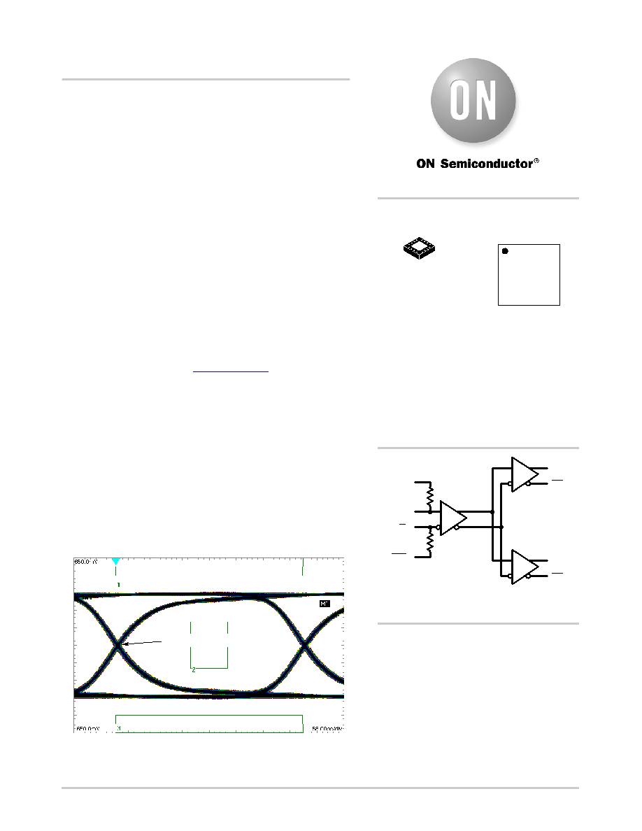
TIME (58 ps/div)
Figure 2. Typical Output Waveform at 2.488 Gb/s with
PRBS 2231 (VINPP = 400 mV; Input Signal DDJ = 14 ps)
VOL
TAGE
(130
mV/div)
Device DDJ = 10 ps
A = Assembly Location
L = Wafer Lot
Y = Year
W = Work Week
G = PbFree Package
*For additional marking information, refer to
Application Note AND8002/D.
MARKING
DIAGRAM*
QFN16
MN SUFFIX
CASE 485G
http://onsemi.com
1
Q0
Q1
D
VTD
Figure 1. Logic Diagram
(Note: Microdot may be in either location)
16
NB6N
11S
ALYW G
G
1
See detailed ordering and shipping information in the package
dimensions section on page 9 of this data sheet.
ORDERING INFORMATION
相关PDF资料 |
PDF描述 |
|---|---|
| MC100LVEP111FARG | IC CLOCK BUFFER MUX 2:10 32-LQFP |
| LTC1663IMS8#TRPBF | IC D/A CONV 10BIT R-R 8-MSOP |
| NB3N551DG | IC CLK BUFFER 1:4 180MHZ 8-SOIC |
| LTC1663IMS8#TR | IC DAC 10BIT R-R MICROPWR 8MSOP |
| MC100LVEP11DR2G | IC CLOCK BUFFER 1:2 3GHZ 8-SOIC |
相关代理商/技术参数 |
参数描述 |
|---|---|
| NB6N11SMNGEVB | 功能描述:BOARD EVAL NB6N11SMNG RoHS:是 类别:编程器,开发系统 >> 评估演示板和套件 系列:* 标准包装:1 系列:PCI Express® (PCIe) 主要目的:接口,收发器,PCI Express 嵌入式:- 已用 IC / 零件:DS80PCI800 主要属性:- 次要属性:- 已供物品:板 |
| NB6N11SMNR2G | 功能描述:时钟缓冲器 NSEB THAI TRANS RoHS:否 制造商:Texas Instruments 输出端数量:5 最大输入频率:40 MHz 传播延迟(最大值): 电源电压-最大:3.45 V 电源电压-最小:2.375 V 最大功率耗散: 最大工作温度:+ 85 C 最小工作温度:- 40 C 封装 / 箱体:LLP-24 封装:Reel |
| NB6N14S | 制造商:ONSEMI 制造商全称:ON Semiconductor 功能描述:3.3 V 1:4 AnyLevel Differential Input to LVDS Fanout Buffer/Translator |
| NB6N14SMNG | 功能描述:时钟缓冲器 HF LVDS FANOUT BUFF/ TRANS RoHS:否 制造商:Texas Instruments 输出端数量:5 最大输入频率:40 MHz 传播延迟(最大值): 电源电压-最大:3.45 V 电源电压-最小:2.375 V 最大功率耗散: 最大工作温度:+ 85 C 最小工作温度:- 40 C 封装 / 箱体:LLP-24 封装:Reel |
| NB6N14SMNGEVB | 功能描述:BOARD EVAL FOR NB6N14SMNG RoHS:是 类别:编程器,开发系统 >> 评估演示板和套件 系列:* 标准包装:1 系列:PCI Express® (PCIe) 主要目的:接口,收发器,PCI Express 嵌入式:- 已用 IC / 零件:DS80PCI800 主要属性:- 次要属性:- 已供物品:板 |
发布紧急采购,3分钟左右您将得到回复。