参数资料
| 型号: | NBSG16VSMNG |
| 厂商: | ON Semiconductor |
| 文件页数: | 7/14页 |
| 文件大小: | 0K |
| 描述: | IC RCVR/DRIVER SIGE DIFF 16QFN |
| 产品变化通告: | Revision of Device Specifications 02/Oct/2008 |
| 标准包装: | 123 |
| 类型: | 收发器 |
| 应用: | 仪表 |
| 安装类型: | 表面贴装 |
| 封装/外壳: | 16-VFQFN 裸露焊盘 |
| 供应商设备封装: | 16-QFN(3x3) |
| 包装: | 管件 |
| 配用: | NBSG16VSBAEVBOS-ND - BOARD EVAL BBG NBSG16VSBA |
| 其它名称: | NBSG16VSMNGOS |
NBSG16VS
http://onsemi.com
2
Figure 1. BGA16 Pinout (Top View)
VEE
D
VTD
VEE
VBB
VTD
NC
VCTRL
VEE
VCC
VMM
VEE
Q
A
B
C
D
12
3
4
VEE NC VCTRL VEE
VEE VBB VMM VEE
VCC
Q
VCC
VTD
D
VTD
56
7
8
16
15
14
13
12
11
10
9
1
2
3
4
NBSG16VS
Exposed Pad (EP)
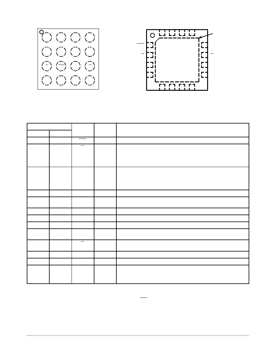
Figure 2. QFN16 Pinout (Top View)
Table 1. PIN DESCRIPTION
Pin
Name
I/O
Description
BGA
QFN
C2
1
VTD
Internal 50 W Termination Pin. See Table 2.
C1
2
D
ECL, CML,
LVCMOS,
LVDS,
LVTTL
Input
Inverted Differential Input. Internal 75 kW to VEE and 36.5 kW to VCC.
B1
3
D
ECL, CML,
LVCMOS,
LVDS,
LVTTL
Input
Noninverted Differential Input. Internal 75 kW to VEE.
B2
4
VTD
Internal 50 W Termination Pin. See Table 2.
A1,D1,A4,
D4
5,8,13,16
VEE
Negative Supply Voltage
A2
6
NC
No Connect
A3
7
VCTRL
Output Amplitude Swing Control. Bypass Pin to VCC through 0.1 mF Capacitor.
B3,C3
9,12
VCC
Positive Supply Voltage
B4
10
Q
RSECL
Output
Noninverted Differential Output. Typically Terminated with 50 W to
VTT = VCC 2 V
C4
11
Q
RSECL
Output
Inverted Differential Output. Typically Terminated with 50 W to VTT = VCC 2 V
D3
14
VMM
LVCMOS Reference Voltage Output. (VCC VEE)/2
D2
15
VBB
ECL Reference Voltage Output
N/A
EP
The Exposed Pad (EP) and the QFN16 package bottom is thermally connected
to the die for improved heat transfer out of package. The exposed pad must be
attached to a heatsinking conduit. The pad is not electrically connected to the
die but may be electrically and thermally connected to VEE on the PC board.
1. The NC pin is electrically connected to the die and must be left open.
2. All VCC and VEE pins must be externally connected to Power Supply to guarantee proper operation. The thermally exposed pad on package
bottom (see case drawing) must be attached to a heatsinking conduit.
3. In the differential configuration when the input termination pins (VTD, VTD) are connected to a common termination voltage, and if no signal
is applied then the device will be susceptible to selfoscillation.
相关PDF资料 |
PDF描述 |
|---|---|
| NBSG16MNG | IC RCVR/DVR RSECL SIGE DF 16QFN |
| NBSG16MMNG | IC RCVR/DVR RSECL SIGE DF 16QFN |
| LFXP3E-5T100C | IC FPGA 3.1KLUTS 62I/O 100-TQFP |
| LFXP3E-5TN100C | IC FPGA 3.1KLUTS 62I/O 100-TQFP |
| LFXP3E-4TN100I | IC FPGA 3.1KLUTS 62I/O 100-TQFP |
相关代理商/技术参数 |
参数描述 |
|---|---|
| NBSG16VSMNHTBG | 功能描述:缓冲器和线路驱动器 BBG 2.5V/3.3V SIGE DIFF RoHS:否 制造商:Micrel 输入线路数量:1 输出线路数量:2 极性:Non-Inverting 电源电压-最大:+/- 5.5 V 电源电压-最小:+/- 2.37 V 最大工作温度:+ 85 C 安装风格:SMD/SMT 封装 / 箱体:MSOP-8 封装:Reel |
| NBSG16VSMNR2 | 功能描述:缓冲器和线路驱动器 2.5V/3.3V SiGe Diff RoHS:否 制造商:Micrel 输入线路数量:1 输出线路数量:2 极性:Non-Inverting 电源电压-最大:+/- 5.5 V 电源电压-最小:+/- 2.37 V 最大工作温度:+ 85 C 安装风格:SMD/SMT 封装 / 箱体:MSOP-8 封装:Reel |
| NBSG16VSMNR2G | 功能描述:缓冲器和线路驱动器 2.5V/3.3V SiGe Diff w/Variable Output RoHS:否 制造商:Micrel 输入线路数量:1 输出线路数量:2 极性:Non-Inverting 电源电压-最大:+/- 5.5 V 电源电压-最小:+/- 2.37 V 最大工作温度:+ 85 C 安装风格:SMD/SMT 封装 / 箱体:MSOP-8 封装:Reel |
| NBSG53A | 制造商:ONSEMI 制造商全称:ON Semiconductor 功能描述:2.5V/3.3V SiGe Selectable Differential Clock and Data D Flip-Flop/Clock Divider with Reset and OLS |
| NBSG53A/D | 制造商:未知厂家 制造商全称:未知厂家 功能描述:2.5V/3.3V SiGe Selectable Differential Clock and Data D Flip-Flop/Clock Divider with Reset and OLS |
发布紧急采购,3分钟左右您将得到回复。