参数资料
| 型号: | NBSG16VSMNR2 |
| 厂商: | ON Semiconductor |
| 文件页数: | 1/14页 |
| 文件大小: | 0K |
| 描述: | IC RCVR/DRIVER SIGE DIFF 16QFN |
| 产品变化通告: | Revision of Device Specifications 02/Oct/2008 LTB Notification 06/Feb/2008 |
| 标准包装: | 3,000 |
| 类型: | 收发器 |
| 应用: | 仪表 |
| 安装类型: | 表面贴装 |
| 封装/外壳: | 16-VFQFN 裸露焊盘 |
| 供应商设备封装: | 16-QFN(3x3) |
| 包装: | 带卷 (TR) |
| 其它名称: | NBSG16VSMNR2OSTR |
Semiconductor Components Industries, LLC, 2008
September, 2008 Rev. 12
1
Publication Order Number:
NBSG16VS/D
NBSG16VS
2.5V/3.3VSiGe Differential
Receiver/Driver with
Variable Output Swing
Description
The NBSG16VS is a differential receiver/driver targeted for high
frequency applications that require variable output swing. The device
is functionally equivalent to the EP16VS device with much higher
bandwidth and lower EMI capabilities. This device may be used for
applications driving VCSEL lasers.
Inputs incorporate internal 50
W termination resistors and accept
NECL (Negative ECL), PECL (Positive ECL), LVTTL, LVCMOS,
CML, or LVDS. The output amplitude is varied by applying a voltage
to the VCTRL input pin. Outputs are variable swing ECL from 100 mV
to 750 mV amplitude, optimized for operation from
VCC VEE = 3.0 V to 3.465 V.
The VBB and VMM pins are internally generated voltage supplies
available to this device only. The VBB is used as a reference voltage
for singleended NECL or PECL inputs and the VMM pin is used as a
reference voltage for LVCMOS inputs. For singleended input
operation, the unused complementary differential input is connected to
VBB or VMM as a switching reference voltage. VBB or VMM may also
rebias ACcoupled inputs. When used, decouple VBB and VMM via a
0.01
mF capacitor and limit current sourcing or sinking to 0.5 mA.
When not used, VBB and VMM outputs should be left open.
Features
Maximum Input Clock Frequency up to 12 GHz Typical
Maximum Input Data Rate up to 12 Gb/s Typical
40 ps Typical Rise and Fall Times (VCTRL = VCC 1 V)
120 ps Typical Propagation Delay (VCTRL = VCC 1 V)
Variable Swing PECL Output with Operating Range: VCC = 2.375 V to
3.465 V with VEE = 0 V
Variable Swing NECL Output with NECL Inputs with
Operating Range: VCC = 0 V with VEE = 2.375 V to 3.465 V
Output Level (100 mV to 750 mV PeaktoPeak Output;
VCC VEE = 3.0 V to 3.465 V), Differential Output Only
50 W Internal Input Termination Resistors
Compatible with Existing 2.5 V/3.3 V EP Devices
VBB and VMM Reference Voltage Output
PbFree Packages are Available
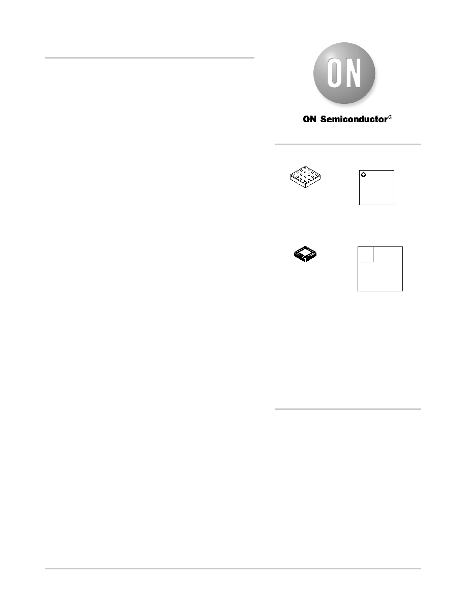
A
= Assembly Location
L
= Wafer Lot
Y
= Year
W
= Work Week
G
= PbFree Package
FCBGA16
BA SUFFIX
CASE 489
MARKING DIAGRAMS*
QFN16
MN SUFFIX
CASE 485G
http://onsemi.com
*For additional marking information, refer to
Application Note AND8002/D.
See detailed ordering and shipping information in the package
dimensions section on page 12 of this data sheet.
ORDERING INFORMATION
(Note: Microdot may be in either location)
SGS
16
ALYWG
G
16
SG
16VS
ALYWG
G
1
相关PDF资料 |
PDF描述 |
|---|---|
| NBSG16VSBAR2 | IC RCVR/DRIVER SIGE DIFF 16FCBGA |
| NBSG16MNR2 | IC RCVR/DRVR RSECL SIGE DF 16QFN |
| LFXP20C-4FN388I | IC FPGA 19.7KLUTS 388FPBGA |
| GBB90DHBS | CONN EDGECARD 180PS R/A .050 SLD |
| LFXP20C-5FN388C | IC FPGA 19.7KLUTS 388FPBGA |
相关代理商/技术参数 |
参数描述 |
|---|---|
| NBSG16VSMNR2G | 功能描述:缓冲器和线路驱动器 2.5V/3.3V SiGe Diff w/Variable Output RoHS:否 制造商:Micrel 输入线路数量:1 输出线路数量:2 极性:Non-Inverting 电源电压-最大:+/- 5.5 V 电源电压-最小:+/- 2.37 V 最大工作温度:+ 85 C 安装风格:SMD/SMT 封装 / 箱体:MSOP-8 封装:Reel |
| NBSG53A | 制造商:ONSEMI 制造商全称:ON Semiconductor 功能描述:2.5V/3.3V SiGe Selectable Differential Clock and Data D Flip-Flop/Clock Divider with Reset and OLS |
| NBSG53A/D | 制造商:未知厂家 制造商全称:未知厂家 功能描述:2.5V/3.3V SiGe Selectable Differential Clock and Data D Flip-Flop/Clock Divider with Reset and OLS |
| NBSG53A_06 | 制造商:ONSEMI 制造商全称:ON Semiconductor 功能描述:2.5V/3.3V SiGe Selectable Differential Clock and Data D Flip−Flop/Clock Divider with Reset and OLS |
| NBSG53ABA | 功能描述:触发器 2.5V/3.3V SiGe Diff RoHS:否 制造商:Texas Instruments 电路数量:2 逻辑系列:SN74 逻辑类型:D-Type Flip-Flop 极性:Inverting, Non-Inverting 输入类型:CMOS 输出类型: 传播延迟时间:4.4 ns 高电平输出电流:- 16 mA 低电平输出电流:16 mA 电源电压-最大:5.5 V 最大工作温度:+ 85 C 安装风格:SMD/SMT 封装 / 箱体:X2SON-8 封装:Reel |
发布紧急采购,3分钟左右您将得到回复。