参数资料
| 型号: | NCN8025MTTBG |
| 厂商: | ON Semiconductor |
| 文件页数: | 15/15页 |
| 文件大小: | 0K |
| 描述: | IC SMART CARD I2C 16-QFN |
| 标准包装: | 1 |
| 系列: | * |
| 其它名称: | NCN8025MTTBGOSDKR |
NCN8025 / NCN8025A
http://onsemi.com
9
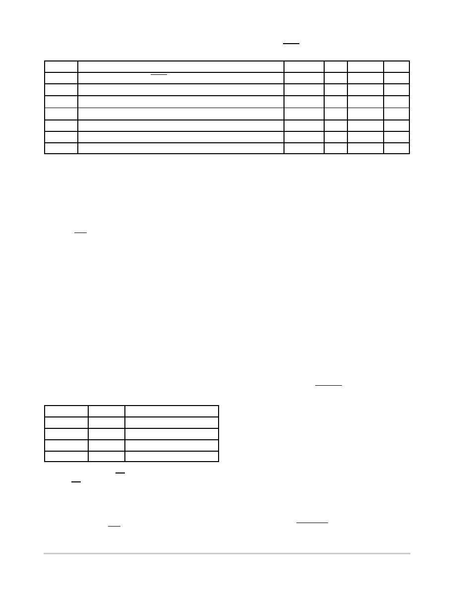
SMART CARD INTERFACE SECTION CI/O, CAUX1, CAUX2, CCLK, CRST, PRES, PRES (VDD = 3.3 V; VDDP = 5 V; Tamb = 25°C;
FCLKIN = 10 MHz)
Symbol
Unit
Max
Typ
Min
Rating
5
8
12
ms
ICI/O
CI/O, CAUX1, CAUX2 current limitation
15
mA
ICCLK
CCLK current limitation
70
mA
ICRST
CRST current limitation
20
mA
Tact
Activation Time (Note 9)
30
100
ms
Tdeact
Deactivation Time (Note 9)
30
250
ms
TempSD
Shutdown temperature (Note 9)
150
°C
9. Guaranteed by design and characterization.
POWER SUPPLY
The NCN8025 / NCN8025A smart card interface has two
power supplies: VDD and VDDP.
VDD is common to the system controller and the interface.
The applied VDD range can go from 2.7 V up to 5.5 V. If VDD
goes below 2.30 V typical (UVLOVDD) a powerdown
sequence is automatically performed. In that case the
interrupt (INT) pin is set Low.
A Low DropOut (LDO) and low noise regulator is used
to provide the 1.8 V, 3 V or 5 V power supply voltage
(CVCC) to the card. VDDP is the LDO’s input voltage.
CVCC is the LDO output. The typical distributed reservoir
output capacitor connected to CVCC is 100 nF + 220 nF. The
capacitor of 100 nF is connected as close as possible to the
CVCC’s pin and the 220 nF one as close as possible to the
card connector C1 pin. Both feature very low ESR values
(lower than 50 m
W). The decoupling capacitors on VDD and
VDDP respectively 100 nF and 10 mF + 100 nF have also to
be connected close to the respective IC pins.
The CVCC pin can source up to 70 mA at 1.8 V, 3 V and
5 V continuously over the VDDP range (see corresponding
specification table), the absolute maximum current being
internally limited below 150 mA (Typical at 120 mA).
The card VCC voltage (CVCC) can be programmed with
the pins VSEL0 and VSEL1 and according to the below table:
Table 1. CVCC PROGRAMMING
VSEL0
VSEL1
CVCC
0
3.0 V
0
1
5.0 V
1
0
3.0 V
1
1.8 V
VSEL0 can be used to select the CVCC programming
mode which can be 5V/3V (VSEL0 connected to Ground)
or 1.8V/3V (VSEL0 connected to VDD). VSEL0 and
VSEL1 are usually programmed before activating the smart
card interface that is when /CMDVCC is High.
There’s no specific sequence for applying VDD or VDDP.
They can be applied to the interface in any sequence. After
powering the device INT pin remains Low until a card is
inserted.
SUPPLY VOLTAGE MONITORING
The supply voltage monitoring block includes the
PowerOn Reset (POR) circuitry and the undervoltage
lockout (UVLO) detection (VDD voltage dropout
detection). PORADJ pin allows the user, according to the
considered application, to adjust the VDD UVLO threshold.
If not used PORADJ pin is connected to Ground
(recommended even if it may be left unconnected).
The input supply voltage is continuously monitored to
prevent under voltage operation. At power up, the system
initializes the internal logic during POR timing and no further
signal can be provided or supported during this period.
The system is ready to operate when the input voltage has
reached the minimum VDD. Considering this, the NCN8025
/ NCN8025A will detect an UnderVoltage situation when
the input supply voltage will drop below 2.30 V typical.
When VDD goes down below the UVLO falling threshold a
deactivation sequence is performed.
The device is inactive during poweron and poweroff of
the VDD supply (8 ms reset pulse).
PORADJ pin is used to modify the UVLO threshold
according to the below relationship considering an external
resistor divider R1 / R2 (see block diagram Figure 1):
UVLO +
R1 ) R2
R2
VPOR
(eq. 1)
If PORADJ is connected to Ground the VDD UVLO
threshold (VDD falling) is typically 2.30 V. In some cases it
can be interesting to adjust this threshold at a higher value
and by the way increase the VDD supply dropout detection
level which enables a deactivation sequence if the VDD
voltage is too low.
For example, there are microcontrollers for which the
minimum supply voltage insuring a correct operating is
higher than 2.6 V; increasing UVLOVDD (VDD falling) is
consequently necessary. Considering for instance a resistor
bridge with R1 = 56 k
W, R2 = 42 kW and VPOR = 1.27 V
typical the VDD dropout detection level can be increased up
to:
UVLO +
56k ) 42k
42k
VPOR + 2.96 V
(eq. 2)
相关PDF资料 |
PDF描述 |
|---|---|
| NCN9252MUTAG | IC USB SWITCH DP3T 12UQFN |
| NCP1092DBRG | IC CTLR IEEE 802.3AF 8-TSSOP |
| NCP1094MNRG | IC INTERFACE CTLR POE-PD 10-DFN |
| NCS36000DG | IC PIR DETECTOR CTLR 14SOIC |
| NCS6415DWR2G | IC VIDEO SWITCH 8X6 20SOIC |
相关代理商/技术参数 |
参数描述 |
|---|---|
| NCN8026A | 制造商:ONSEMI 制造商全称:ON Semiconductor 功能描述:Compact Low Power Smart Card Interface IC |
| NCN8026AMNGEVB | 制造商:ON Semiconductor 功能描述:NCN8026A QFN24L EVAL BD - Bulk 制造商:ON Semiconductor 功能描述:Interface Development Tools NCN8026A QFN24L Smart Card IF |
| NCN8026AMNTXG | 制造商:ON Semiconductor 功能描述:SMART CARD IC IN QFN 24L - Tape and Reel |
| NCN8-18GM40-N0-V1 | 制造商:PEPPERL+FUCHS 功能描述:Inductive Sensors - NAMUR 制造商:Pepperl+Fuchs 功能描述:Bulk |
| NCN8-18GM40-Z0 | 制造商:PEPPERL+FUCHS 功能描述:Inductive DC |
发布紧急采购,3分钟左右您将得到回复。