参数资料
| 型号: | NCN8025MTTBG |
| 厂商: | ON Semiconductor |
| 文件页数: | 2/15页 |
| 文件大小: | 0K |
| 描述: | IC SMART CARD I2C 16-QFN |
| 标准包装: | 1 |
| 系列: | * |
| 其它名称: | NCN8025MTTBGOSDKR |
NCN8025 / NCN8025A
http://onsemi.com
10
CLOCK DIVIDER:
The input clock can be divided by 1/1, 1/2, 1/4, or 1/8,
depending upon the specific application, prior to be applied
to the smart card driver. These division ratios are
programmed using pins CLKDIV1 and CLKDIV2 (see
Table 2). The input clock is provided externally to pin
CLKIN.
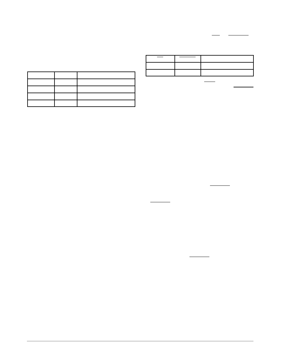
Table 2. CLOCK FREQUENCY PROGRAMMING
CLKDIV1
CLKDIV2
FCCLK
0
CLKIN / 8
0
1
CKLKIN / 4
1
0
CLKIN
1
CLKIN / 2
The clock input stage (CLKIN) can handle a 27 MHz
maximum frequency signal. Of course, the ratio must be
defined by the user to cope with Smart Card considered in
a given application
In order to avoid any duty cycle out of the 45% / 55%
range specification, the divider is synchronized by the last
flip flop, thus yielding a constant 50% duty cycle, whatever
be the divider ratio 1/2, 1/4 or 1/8. On the other hand, the
output signal Duty Cycle cannot be guaranteed 50% if the
division ratio is 1 and if the input Duty Cycle signal is not
within the 46% 56% range at the CLKIN input.
When the signal applied to CLKIN is coming from the
external controller, the clock will be applied to the card
under the control of the microcontroller or similar device
after the activation sequence has been completed.
DATA I/O, AUX1 and AUX2 LEVEL SHIFTERS
The three bidirectional level shifters I/O, AUX1 and
AUX2 adapt the voltage difference that might exist between
the microcontroller and the smart card. These three
channels are identical. The first side of the bidirectional
level shifter dropping Low (falling edge) becomes the driver
side until the level shifter enters again in the idle state pulling
High CI/O and I/Ouc.
Passive 11 k
W pullup resistors have been internally
integrated on each terminal of the bidirectional channel. In
addition with these pullup resistors, an active pullup
circuit provides a fast charge of the stray capacitance.
The current to and from the card I/O lines is limited
internally to 15 mA and the maximum guaranteed frequency
on these lines is 1 MHz.
STANDBY MODE
After a Poweron reset, the circuit enters the standby mode.
A minimum number of circuits are active while waiting for
the microcontroller to start a session:
All card contacts are inactive
Pins I/Ouc, AUX1uc and AUX2uc are in the
highimpedance state (11 k
W pullup resistor to VDD)
Card pins are inactive and pulled Low
Supply Voltage monitoring is active
POWERUP
In the standby mode the microcontroller can check the
presence of a card using the signals INT and CMDVCC as
shown in Table 3:
Table 3. CARD PRESENCE STATE
INT
CMDVCC
State
HIGH
Card present
LOW
HIGH
Card not present
If a card is detected present (PRES or PRES active) the
controller can start a card session by pulling CMDVCC
Low. Card activation is run (t0, Figure 6). This PowerUp
Sequence makes sure all the card related signals are LOW
during the CVCC positive going slope. These lines are
validated when CVCC is stable and above the minimum
voltage specified. When the CVCC voltage reaches the
programmed value (1.8 V, 3.0 V or 5.0 V), the circuit
activates the card signals according to the following
sequence (Figure 6):
CVCC is poweredup at its nominal value (t1)
I/O, AUX1 and AUX2 lines are activated (t2)
Then Clock is activated and the clock signal is applied
to the card (typically 500 ns after I/Os lines) (t3)
Finally the Reset level shifter is enabled (typically
500 ns after clock channel) (t4)
The clock can also be applied to the card using a RSTIN
mode allowing controlling the clock starting by setting
RSTIN Low (Figure 5). Before running the activation
sequence, that is before setting Low CMDVCC RSTIN is set
High. The following sequence is applied:
The Smart Card Interface is enable by setting
CMDVCC LOW (RSTIN is High).
Between t2 (Figure 5) and t5 = 200
ms, RSTIN is reset
to LOW and CCLK will start precisely at this moment
allowing a precise count of clock cycles before toggling
CRST Low to High for ATR (Answer To Reset)
request.
CRST remains LOW until 200
ms; after t5 = 200 ms
CRST is enabled and is the copy of RSTIN which has
no more control on the clock.
If controlling the clock with RSTIN is not necessary
(Normal Mode), then CMDVCC can be set LOW with
RSTIN LOW. In that case, CLK will start minimum 500 ns
after the transition on I/O (Figure 6), and to obtain an ATR,
CRST can be set High by RSTIN also about 500 ns after the
clock channel activation (Tact).
The internal activation sequence activates the different
channels according to a specific hardware builtin
sequencing internally defined but at the end the actual
activation sequencing is the responsibility of the application
software and can be redefined by the microcontroller to
comply with the different standards and the different ways
the standards manage this activation (for example light
differences exist between the EMV and the ISO7816
standards).
相关PDF资料 |
PDF描述 |
|---|---|
| NCN9252MUTAG | IC USB SWITCH DP3T 12UQFN |
| NCP1092DBRG | IC CTLR IEEE 802.3AF 8-TSSOP |
| NCP1094MNRG | IC INTERFACE CTLR POE-PD 10-DFN |
| NCS36000DG | IC PIR DETECTOR CTLR 14SOIC |
| NCS6415DWR2G | IC VIDEO SWITCH 8X6 20SOIC |
相关代理商/技术参数 |
参数描述 |
|---|---|
| NCN8026A | 制造商:ONSEMI 制造商全称:ON Semiconductor 功能描述:Compact Low Power Smart Card Interface IC |
| NCN8026AMNGEVB | 制造商:ON Semiconductor 功能描述:NCN8026A QFN24L EVAL BD - Bulk 制造商:ON Semiconductor 功能描述:Interface Development Tools NCN8026A QFN24L Smart Card IF |
| NCN8026AMNTXG | 制造商:ON Semiconductor 功能描述:SMART CARD IC IN QFN 24L - Tape and Reel |
| NCN8-18GM40-N0-V1 | 制造商:PEPPERL+FUCHS 功能描述:Inductive Sensors - NAMUR 制造商:Pepperl+Fuchs 功能描述:Bulk |
| NCN8-18GM40-Z0 | 制造商:PEPPERL+FUCHS 功能描述:Inductive DC |
发布紧急采购,3分钟左右您将得到回复。