- 您现在的位置:买卖IC网 > PDF目录17227 > NCP1216AFORWEVB (ON Semiconductor)BOARD EVAL NCP1216A DC/DC CONV PDF资料下载
参数资料
| 型号: | NCP1216AFORWEVB |
| 厂商: | ON Semiconductor |
| 文件页数: | 12/18页 |
| 文件大小: | 0K |
| 描述: | BOARD EVAL NCP1216A DC/DC CONV |
| 产品变化通告: | 1Q2012 Discontinuation 30/Mar/2012 |
| 设计资源: | NCP1216AFORWEVB Schematic NCP1216AFORWEVB Bill of Materials NCP1216AFORWEVB Test Procedure NCP1216AFORWEVB Gerber Zip |
| 标准包装: | 1 |
| 系列: | * |
| 其它名称: | NCP1216AFORWEVB-ND NCP1216AFORWEVBOS |
�� �
�
�NCP1216,� NCP1216A�
�300�
�Max� Peak�
�Current�
�due� to� the� DSS� operation.� In� our� example,� at�
�T� ambient� =� 50� °� C,� I� CC2� is� measured� to� be� 2.9� mA� with� a�
�10� A� /� 600� V� MOSFET.� As� a� result,� the� NCP1216� will�
�350� V�
�2.9� mA@TA� +� 50� C� +� 1� W�
�200�
�Skip� Cycle�
�Current� Limit�
�dissipate� from� a� 250� VAC� network,�
�°�
�(eq.� 11)�
�P� max� +� Jmax�
�+� 1W�
�T� *� TAmax�
�R� q� J� *� A�
�Vbulkmin� *� 50� V�
�Rdrop� v�
�100�
�0�
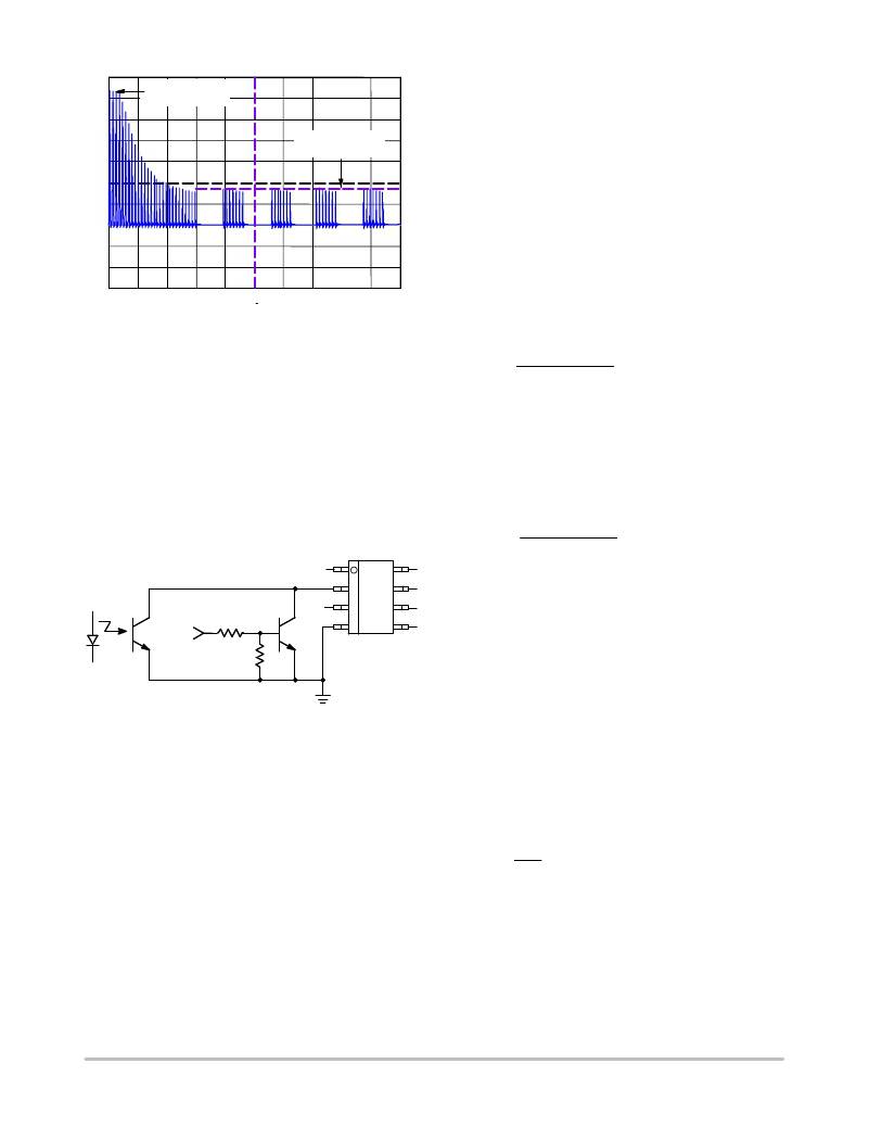
�315.4U� 882.7U� 1.450M� 2.017M� 2.585M�
�Figure� 23.� The� Skip� Cycle� Takes� Place� at� Low� Peak�
�Currents� which� Guarantees� Noise� Free� Operation�
�Non� ?� Latching� Shutdown�
�In� some� cases,� it� might� be� desirable� to� shut� off� the� part�
�temporarily� and� authorize� its� restart� once� the� default� has�
�disappeared.� This� option� can� easily� be� accomplished�
�through� a� single� NPN� bipolar� transistor� wired� between� FB�
�and� ground.� By� pulling� FB� below� the� Adj� pin� 1� level,� the�
�output� pulses� are� disabled� as� long� as� FB� is� pulled� below�
�pin� 1.� As� soon� as� FB� is� relaxed,� the� IC� resumes� its� operation.�
�Figure� 24� depicts� the� application� example:�
�The� PDIP� ?� 7� package� offers� a� junction� ?� to� ?� ambient� thermal�
�resistance� R� q� J� ?� A� of� 100� °� C/W.� Adding� some� copper� area�
�around� the� PCB� footprint� will� help� decreasing� this� number:�
�12� mm� x� 12� mm� to� drop� R� q� J� ?� A� down� to� 75� °� C/W� with� 35� m�
�copper� thickness� (1� oz.)� or� 6.5� mm� x� 6.5� mm� with� 70� m�
�copper� thickness� (2� oz.).� For� a� SOIC� ?� 8,� the� original�
�178� °� C/W� will� drop� to� 100� °� C/W� with� the� same� amount� of�
�copper.� With� this� later� PDIP� ?� 7� number,� we� can� compute� the�
�maximum� power� dissipation� that� the� package� accepts� at� an�
�ambient� of� 50� °� C:�
�(eq.� 12)�
�which� barely� matches� our� previous� budget.� Several�
�solutions� exist� to� help� improving� the� situation:�
�1.� Insert� a� Resistor� in� Series� with� Pin� 8:� This� resistor� will�
�take� a� part� of� the� heat� normally� dissipated� by� the� NCP1216.�
�Calculations� of� this� resistor� imply� that� V� pin8� does� not� drop�
�below� 30� V� in� the� lowest� mains� conditions.� Therefore,� R� drop�
�can� be� selected� with:�
�(eq.� 13)�
�8� mA�
�ON/OFF�
�Q1�
�1�
�2�
�3�
�4�
�8�
�7�
�6�
�5�
�In� our� case,� V� bulk� minimum� is� 120� VDC,� which� leads� to� a�
�dropping� resistor� of� 8.7� k� W� .� With� the� above� example� in�
�mind,� the� DSS� will� exhibit� a� duty� ?� cycle� of:�
�2.9� mA� 8� mA� +� 36%� (eq.� 14)�
�By� inserting� the� 8.7� k� W� resistor,� we� drop�
�8.7� k� W� *� 8� mA� +� 69.6� V�
�(eq.� 15)�
�during� the� DSS� activation.� The� power� dissipated� by� the�
�Figure� 24.� Another� Way� of� Shutting� Down� the� IC�
�without� a� Definitive� Latchoff� State�
�NCP1216� is� therefore:�
�Pinstant� *� DSSduty� *� cycle� +�
�(350� *� 69)� *� 8� m� *� 0.36� +� 800� mW�
�(eq.� 16)�
�A� full� latching� shutdown,� including� overtemperature�
�We� can� pass� the� limit� and� the� resistor� will� dissipate�
�protection,� is� described� in� application� note� AND8069/D.�
�1� W� *� 800� mW� +� 200� mW�
�(eq.� 17)�
�(VHVDC� *� 11� V)� ICC2�
�pdrop� +� 69�
�2�
�Power� Dissipation�
�The� NCP1216� is� directly� supplied� from� the� DC� rail�
�through� the� internal� DSS� circuitry.� The� current� flowing�
�through� the� DSS� is� therefore� the� direct� image� of� the�
�NCP1216� current� consumption.� The� total� power� dissipation�
�can� be� evaluated� using:�
�(eq.� 10)�
�which� is,� as� we� saw,� directly� related� to� the� MOSFET� Q� g� .� If�
�we� operate� the� device� on� a� 90� ?� 250� VAC� rail,� the� maximum�
�or�
�*� 0.36� (eq.� 18)�
�8.7� k�
�2.� Select� a� MOSFET� with� a� Lower� Q� g� :� Certain� MOSFETs�
�exhibit� different� total� gate� charges� depending� on� the�
�technology� they� use.� Careful� selection� of� this� component�
�can� help� to� significantly� decrease� the� dissipated� heat.�
�rectified� voltage� can� go� up� to� 350� VDC.� However,� as� the�
�characterization� curves� show,� the� current� consumption�
�drops� at� a� higher� junction� temperature,� which� quickly� occurs�
�http://onsemi.com�
�12�
�相关PDF资料 |
PDF描述 |
|---|---|
| 594D337X96R3C8T | CAP TANT 330UF 6.3V 10% 2812 |
| GI1402HE3/45 | DIODE 8A 100V 35NS SGL TO220-2 |
| GEC17DRYH-S13 | CONN EDGECARD 34POS .100 EXTEND |
| EBM15DCTD-S288 | CONN EDGECARD 30POS .156 EXTEND |
| HCM06DSEN-S243 | CONN EDGECARD 12POS .156 EYELET |
相关代理商/技术参数 |
参数描述 |
|---|---|
| NCP1216AFORWGEVB | 功能描述:BOARD EVAL NCP1216A 35W RoHS:是 类别:编程器,开发系统 >> 评估板 - LED 驱动器 系列:* 标准包装:1 系列:PowerWise® 电流 - 输出 / 通道:20mA 输出及类型:1,非隔离 输出电压:17V 特点:可调光 输入电压:2.7 ~ 5.5 V 已供物品:板 已用 IC / 零件:LM3508 相关产品:LM3508TLX-ND - IC LED DRVR WHT BCKLGT 9USMDLM3508TLDKR-ND - IC LED DRVR WHT BCKLGT 9MICROSMDLM3508TLCT-ND - IC LED DRVR WHT BCKLGT 9MICROSMDLM3508TLTR-ND - IC LED DRVR WHT BCKLGT 9MICROSMD |
| NCP1216AP100 | 功能描述:开关变换器、稳压器与控制器 Current Mode PWM RoHS:否 制造商:Texas Instruments 输出电压:1.2 V to 10 V 输出电流:300 mA 输出功率: 输入电压:3 V to 17 V 开关频率:1 MHz 工作温度范围: 安装风格:SMD/SMT 封装 / 箱体:WSON-8 封装:Reel |
| NCP1216AP100G | 功能描述:电流型 PWM 控制器 Current Mode PWM w/50% Duty Cycle Max RoHS:否 制造商:Texas Instruments 开关频率:27 KHz 上升时间: 下降时间: 工作电源电压:6 V to 15 V 工作电源电流:1.5 mA 输出端数量:1 最大工作温度:+ 105 C 安装风格:SMD/SMT 封装 / 箱体:TSSOP-14 |
| NCP1216AP133 | 功能描述:电流型 PWM 控制器 Current Mode PWM RoHS:否 制造商:Texas Instruments 开关频率:27 KHz 上升时间: 下降时间: 工作电源电压:6 V to 15 V 工作电源电流:1.5 mA 输出端数量:1 最大工作温度:+ 105 C 安装风格:SMD/SMT 封装 / 箱体:TSSOP-14 |
| NCP1216AP133G | 功能描述:电流型 PWM 控制器 Current Mode PWM w/50% Duty Cycle Max RoHS:否 制造商:Texas Instruments 开关频率:27 KHz 上升时间: 下降时间: 工作电源电压:6 V to 15 V 工作电源电流:1.5 mA 输出端数量:1 最大工作温度:+ 105 C 安装风格:SMD/SMT 封装 / 箱体:TSSOP-14 |
发布紧急采购,3分钟左右您将得到回复。