- 您现在的位置:买卖IC网 > PDF目录17227 > NCP1216AFORWEVB (ON Semiconductor)BOARD EVAL NCP1216A DC/DC CONV PDF资料下载
参数资料
| 型号: | NCP1216AFORWEVB |
| 厂商: | ON Semiconductor |
| 文件页数: | 14/18页 |
| 文件大小: | 0K |
| 描述: | BOARD EVAL NCP1216A DC/DC CONV |
| 产品变化通告: | 1Q2012 Discontinuation 30/Mar/2012 |
| 设计资源: | NCP1216AFORWEVB Schematic NCP1216AFORWEVB Bill of Materials NCP1216AFORWEVB Test Procedure NCP1216AFORWEVB Gerber Zip |
| 标准包装: | 1 |
| 系列: | * |
| 其它名称: | NCP1216AFORWEVB-ND NCP1216AFORWEVBOS |
�� �
�
�NCP1216,� NCP1216A�
�D� t� +� D� V·C� (eq.� 19)�
�depends� on� the� startup� sequence� of� your� system,� i.e.� when�
�you� first� apply� the� power� to� the� IC.� The� corresponding�
�transient� fault� duration� due� to� the� output� capacitor� charging�
�must� be� less� than� the� time� needed� to� discharge� from� 12.2� V�
�to� 10� V,� otherwise� the� supply� will� not� properly� start.� The� test�
�consists� in� either� simulating� or� measuring� in� the� lab� how�
�much� time� the� system� takes� to� reach� the� regulation� at� full�
�load.� Let’s� suppose� that� this� time� corresponds� to� 6ms.�
�Therefore� a� V� CC� fall� time� of� 10� ms� could� be� well�
�appropriated� in� order� to� not� trigger� the� overload� detection�
�circuitry.� If� the� corresponding� IC� consumption,� including�
�the� MOSFET� drive,� establishes� at� 2.9� mA,� we� can� calculate�
�the� required� capacitor� using� the� following� formula:�
�i�
�with� D� V� =� 2.2� V.� Then� for� a� wanted� D� t� of� 30� ms,� C� equals�
�39.5� m� F� or� a� 68� m� F� for� a� standard� value� (including� ±� 20%�
�dispersions).� When� an� overload� condition� occurs,� the� IC�
�blocks� its� internal� circuitry� and� its� consumption� drops� to�
�350� m� A� typical.� This� happens� at� V� CC� =� 10� V� and� it� remains�
�stuck� until� V� CC� reaches� 5.6� V:� we� are� in� latchoff� phase.�
�Again,� using� the� selected� 68� m� F� and� 350� m� A� current�
�consumption,� this� latchoff� phase� lasts:� 780� ms.�
�Protecting� the� Controller� Against� Negative� Spikes�
�As� with� any� controller� built� upon� a� CMOS� technology,� it�
�is� the� designer� ’s� duty� to� avoid� the� presence� of� negative�
�spikes� on� sensitive� pins.� Negative� signals� have� the� bad� habit�
�to� forward� bias� the� controller� substrate� and� induce� erratic�
�behaviors.� Sometimes,� the� injection� can� be� so� strong� that�
�internal� parasitic� SCRs� are� triggered,� engendering�
�irremediable� damages� to� the� IC� if� a� low� impedance� path� is�
�offered� between� V� CC� and� GND.� If� the� current� sense� pin� is�
�often� the� seat� of� such� spurious� signals,� the� high� ?� voltage� pin�
�can� also� be� the� source� of� problems� in� certain� circumstances.�
�During� the� turn� ?� off� sequence,� e.g.� when� the� user� unplugs� the�
�power� supply,� the� controller� is� still� fed� by� its� V� CC� capacitor�
�and� keeps� activating� the� MOSFET� ON� and� OFF� with� a� peak�
�current� limited� by� R� sense� .� Unfortunately,� if� the� quality�
�coefficient� Q� of� the� resonating� network� formed� by� L� p� and�
�C� bulk� is� low� (e.g.� the� MOSFET� R� dson� +� R� sense� are� small),�
�conditions� are� met� to� make� the� circuit� resonate� and� thus�
�negatively� bias� the� controller.� Since� we� are� talking� about� ms�
�pulses,� the� amount� of� injected� charge,� (Q� =� I� *� t),�
�immediately� latches� the� controller� that� brutally� discharges�
�its� V� CC� capacitor.� If� this� V� CC� capacitor� is� of� sufficient� value,�
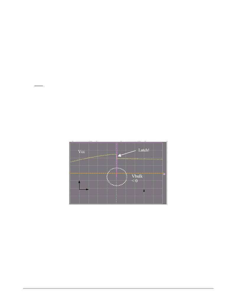
�its� stored� energy� damages� the� controller.� Figure� 26� depicts�
�a� typical� negative� shot� occurring� on� the� HV� pin� where� the�
�brutal� V� CC� discharge� testifies� for� latchup.�
�0�
�V� CC�
�5� V/DIV�
�10� ms/DIV�
�V� latch�
�1� V/DIV�
�Figure� 26.� A� Negative� Spike� Takes� Place� on� the� Bulk� Capacitor� at� the� Switch� ?� off� Sequence�
�Simple� and� inexpensive� cures� exist� to� prevent� from�
�internal� parasitic� SCR� activation.� One� of� them� consists� in�
�inserting� a� resistor� in� series� with� the� high� ?� voltage� pin� to�
�keep� the� negative� current� to� the� lowest� when� the� bulk�
�becomes� negative� (Figure� 27).� Please� note� that� the� negative�
�Another� option� (Figure� 28)� consists� in� wiring� a� diode�
�from� V� CC� to� the� bulk� capacitor� to� force� V� CC� to� reach�
�VCC� ON� sooner� and� thus� stops� the� switching� activity� before�
�the� bulk� capacitor� gets� deeply� discharged.� For� security�
�reasons,� two� diodes� can� be� connected� in� series.�
�spike� is� clamped� to� (� ?� 2� *� V� f� )� due� to� the� diode� bridge.� Also,�
�the� power� dissipation� of� this� resistor� is� extremely� small� since�
�it� only� heats� up� during� the� startup� sequence.�
�http://onsemi.com�
�14�
�相关PDF资料 |
PDF描述 |
|---|---|
| 594D337X96R3C8T | CAP TANT 330UF 6.3V 10% 2812 |
| GI1402HE3/45 | DIODE 8A 100V 35NS SGL TO220-2 |
| GEC17DRYH-S13 | CONN EDGECARD 34POS .100 EXTEND |
| EBM15DCTD-S288 | CONN EDGECARD 30POS .156 EXTEND |
| HCM06DSEN-S243 | CONN EDGECARD 12POS .156 EYELET |
相关代理商/技术参数 |
参数描述 |
|---|---|
| NCP1216AFORWGEVB | 功能描述:BOARD EVAL NCP1216A 35W RoHS:是 类别:编程器,开发系统 >> 评估板 - LED 驱动器 系列:* 标准包装:1 系列:PowerWise® 电流 - 输出 / 通道:20mA 输出及类型:1,非隔离 输出电压:17V 特点:可调光 输入电压:2.7 ~ 5.5 V 已供物品:板 已用 IC / 零件:LM3508 相关产品:LM3508TLX-ND - IC LED DRVR WHT BCKLGT 9USMDLM3508TLDKR-ND - IC LED DRVR WHT BCKLGT 9MICROSMDLM3508TLCT-ND - IC LED DRVR WHT BCKLGT 9MICROSMDLM3508TLTR-ND - IC LED DRVR WHT BCKLGT 9MICROSMD |
| NCP1216AP100 | 功能描述:开关变换器、稳压器与控制器 Current Mode PWM RoHS:否 制造商:Texas Instruments 输出电压:1.2 V to 10 V 输出电流:300 mA 输出功率: 输入电压:3 V to 17 V 开关频率:1 MHz 工作温度范围: 安装风格:SMD/SMT 封装 / 箱体:WSON-8 封装:Reel |
| NCP1216AP100G | 功能描述:电流型 PWM 控制器 Current Mode PWM w/50% Duty Cycle Max RoHS:否 制造商:Texas Instruments 开关频率:27 KHz 上升时间: 下降时间: 工作电源电压:6 V to 15 V 工作电源电流:1.5 mA 输出端数量:1 最大工作温度:+ 105 C 安装风格:SMD/SMT 封装 / 箱体:TSSOP-14 |
| NCP1216AP133 | 功能描述:电流型 PWM 控制器 Current Mode PWM RoHS:否 制造商:Texas Instruments 开关频率:27 KHz 上升时间: 下降时间: 工作电源电压:6 V to 15 V 工作电源电流:1.5 mA 输出端数量:1 最大工作温度:+ 105 C 安装风格:SMD/SMT 封装 / 箱体:TSSOP-14 |
| NCP1216AP133G | 功能描述:电流型 PWM 控制器 Current Mode PWM w/50% Duty Cycle Max RoHS:否 制造商:Texas Instruments 开关频率:27 KHz 上升时间: 下降时间: 工作电源电压:6 V to 15 V 工作电源电流:1.5 mA 输出端数量:1 最大工作温度:+ 105 C 安装风格:SMD/SMT 封装 / 箱体:TSSOP-14 |
发布紧急采购,3分钟左右您将得到回复。