- 您现在的位置:买卖IC网 > PDF目录22150 > NCP1351BDR2G (ON Semiconductor)IC CTLR PWM VAR-OFF TIME 8-SOIC PDF资料下载
参数资料
| 型号: | NCP1351BDR2G |
| 厂商: | ON Semiconductor |
| 文件页数: | 14/27页 |
| 文件大小: | 0K |
| 描述: | IC CTLR PWM VAR-OFF TIME 8-SOIC |
| 标准包装: | 1 |
| 输出隔离: | 隔离 |
| 频率范围: | 调节 |
| 输入电压: | 9.5 V ~ 28 V |
| 工作温度: | -25°C ~ 125°C |
| 封装/外壳: | 8-SOIC(0.154",3.90mm 宽) |
| 供应商设备封装: | 8-SOICN |
| 包装: | 标准包装 |
| 其它名称: | NCP1351BDR2GOSDKR |
第1页第2页第3页第4页第5页第6页第7页第8页第9页第10页第11页第12页第13页当前第14页第15页第16页第17页第18页第19页第20页第21页第22页第23页第24页第25页第26页第27页
�� �
�
�NCP1351�
�V� CC�
�C� t�
�270p� V� CC�
�C� t�
�IC� t�
�10� m�
�Reset�
�V� offset�
�FB�
�I� FB�
�I� FB�
�500mV�
�-�
�Clock�
�+�
�+�
�C1�
�100n�
�R1�
�2.5k�
�D� FB�
�I� FB�
�R� FB�
�45k�
�V� CC�
�C3�
�22pF�
�CS�
�ICS� min�
�I� diff�
�I� diff�
�I� diff� =� ICS� max� -� ICS� min�
�R� offset�
�3.9k�
�to� R� sense�
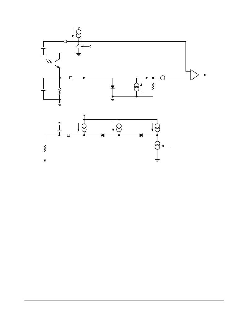
�Figure� 15.� The� Feedback� Section� Inside� the� NCP1351�
�f� (IFB)�
�The� FB� pin� can� actually� be� seen� as� a� diode,� forward� biased�
�by� the� optocoupler� current.� The� feedback� current,� I� FB� on�
�Figure� 15,� enter� an� internal� 45� k� W� resistor� which� develops�
�a� voltage.� This� voltage� becomes� the� variable� threshold� point�
�for� the� capacitor� charge,� as� indicated� by� Figure� 10.� Thus,� in�
�lack� of� feedback� current� (start-up� or� short-circuit),� there� is�
�no� voltage� across� the� 45� k� W� and� the� series� offset� of� 500� mV�
�clamps� the� capacitor� swing.� If� a� 270� pF� capacitor� is� used,� the�
�maximum� switching� frequency� is� 65� kHz.�
�Folding� the� frequency� back� at� a� rather� high� peak� current�
�can� obviously� generate� audible� noise.� For� this� reason,� the�
�NCP1351� uses� a� patented� current� compression� technique�
�which� reduces� the� peak� current� in� lighter� load� conditions.� By�
�load� conditions,� the� feedback� current� is� weak� and� all� the�
�current� flowing� through� the� external� offset� resistor� is:�
�ICS� +� ICS_min� )� Idif� +� ICS_max� *� ICS_min� )� ICS_min�
�+� ICS_max� (eq.� 13)�
�As� the� load� goes� lighter,� the� feedback� current� increases� and�
�starts� to� steal� current� away� from� the� generators.� Equation� 12�
�can� thus� be� updated� by:�
�ICS� +� ICS_max� *� kIFB� (eq.� 14)�
�Equation� 13� testifies� for� the� current� reduction� on� the� offset�
�generator,� k� represents� an� internal� coefficient.� When� the�
�feedback� current� equals� I� dif� ,� the� offset� becomes:�
�design,� the� peak� current� changes� from� 100%� of� its� full� load�
�ICS� +� ICS_min�
�(eq.� 15)�
�value,� to� 30%� of� this� value� in� light� load� conditions.� This� is�
�the� block� placed� on� the� lower� left� corner� of� Figure� 15.� In� full�
�http://onsemi.com�
�14�
�相关PDF资料 |
PDF描述 |
|---|---|
| VI-JW3-CW-B1 | CONVERTER MOD DC/DC 24V 100W |
| AMC15DRAI | CONN EDGECARD 30POS .100 R/A DIP |
| RCM06DRMI-S288 | CONN EDGECARD 12POS .156 EXTEND |
| ACB50DHLT | CONN EDGECARD 100PS .050 DIP SLD |
| VI-J1M-CW-B1 | CONVERTER MOD DC/DC 10V 100W |
相关代理商/技术参数 |
参数描述 |
|---|---|
| NCP1351BPG | 功能描述:电流型 PWM 控制器 VRIABLE OFF TM CNTRL RoHS:否 制造商:Texas Instruments 开关频率:27 KHz 上升时间: 下降时间: 工作电源电压:6 V to 15 V 工作电源电流:1.5 mA 输出端数量:1 最大工作温度:+ 105 C 安装风格:SMD/SMT 封装 / 箱体:TSSOP-14 |
| NCP1351CDR2G | 功能描述:电流型 PWM 控制器 PWM CONTROLLER RoHS:否 制造商:Texas Instruments 开关频率:27 KHz 上升时间: 下降时间: 工作电源电压:6 V to 15 V 工作电源电流:1.5 mA 输出端数量:1 最大工作温度:+ 105 C 安装风格:SMD/SMT 封装 / 箱体:TSSOP-14 |
| NCP1351CPG | 功能描述:电流型 PWM 控制器 VRIABLE OFF TM CNTRL RoHS:否 制造商:Texas Instruments 开关频率:27 KHz 上升时间: 下降时间: 工作电源电压:6 V to 15 V 工作电源电流:1.5 mA 输出端数量:1 最大工作温度:+ 105 C 安装风格:SMD/SMT 封装 / 箱体:TSSOP-14 |
| NCP1351DDR2G | 功能描述:电流型 PWM 控制器 PWM CONTROLLER RoHS:否 制造商:Texas Instruments 开关频率:27 KHz 上升时间: 下降时间: 工作电源电压:6 V to 15 V 工作电源电流:1.5 mA 输出端数量:1 最大工作温度:+ 105 C 安装风格:SMD/SMT 封装 / 箱体:TSSOP-14 |
| NCP1351DPG | 功能描述:电流型 PWM 控制器 VRIABLE OFF TM CNTRL RoHS:否 制造商:Texas Instruments 开关频率:27 KHz 上升时间: 下降时间: 工作电源电压:6 V to 15 V 工作电源电流:1.5 mA 输出端数量:1 最大工作温度:+ 105 C 安装风格:SMD/SMT 封装 / 箱体:TSSOP-14 |
发布紧急采购,3分钟左右您将得到回复。