- 您现在的位置:买卖IC网 > PDF目录22150 > NCP1351BDR2G (ON Semiconductor)IC CTLR PWM VAR-OFF TIME 8-SOIC PDF资料下载
参数资料
| 型号: | NCP1351BDR2G |
| 厂商: | ON Semiconductor |
| 文件页数: | 19/27页 |
| 文件大小: | 0K |
| 描述: | IC CTLR PWM VAR-OFF TIME 8-SOIC |
| 标准包装: | 1 |
| 输出隔离: | 隔离 |
| 频率范围: | 调节 |
| 输入电压: | 9.5 V ~ 28 V |
| 工作温度: | -25°C ~ 125°C |
| 封装/外壳: | 8-SOIC(0.154",3.90mm 宽) |
| 供应商设备封装: | 8-SOICN |
| 包装: | 标准包装 |
| 其它名称: | NCP1351BDR2GOSDKR |
第1页第2页第3页第4页第5页第6页第7页第8页第9页第10页第11页第12页第13页第14页第15页第16页第17页第18页当前第19页第20页第21页第22页第23页第24页第25页第26页第27页
��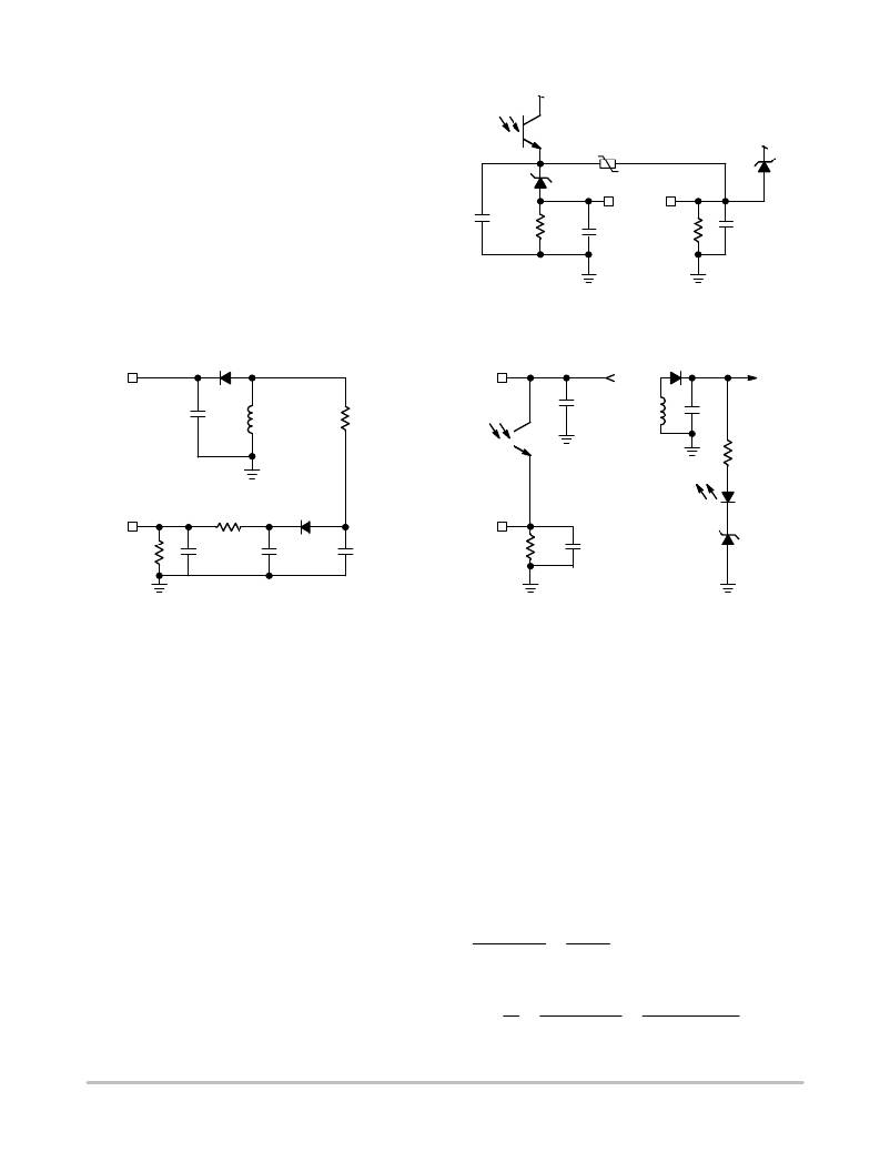 �
�
�NCP1351�
�Latch� Input�
�The� NCP1351� features� a� patented� circuitry� which�
�prevents� the� FB� input� to� be� of� low� impedance� before� the� V� CC�
�reaches� the� VCC� ON� level.� As� such,� the� circuit� can� work� in�
�a� primary� regulation� scheme.� Capitalizing� on� this� typical�
�V� CC�
�OVP�
�D2�
�option,� Figure� 24� shows� how� to� insert� a� zener� diode� in� series�
�with� the� optocoupler� emitter� pin.� In� that� way,� the� current�
�5V�
�FB�
�Latch�
�biases� the� zener� diode� and� offers� a� nice� reference� voltage,�
�appearing� at� the� loop� closure� (e.g.� when� the� output� reaches�
�the� target).� Yes,� you� can� use� this� reference� voltage� to� supply�
�C2�
�100n�
�R1�
�2.5k�
�C1�
�100nF�
�R� pulldown�
�C3�
�100nF�
�a� NTC� and� form� a� cheap� OTP� protection.�
�Figure� 24.� The� Latch� Input� Offers� Everything� Needed�
�to� Implement� an� OTP� Circuit.� Another� Zener� Can�
�Help� combining� an� OVP� Circuit� if� Necessary�
�V� CC�
�V� CC�
�Aux�
�OUT�
�CV� CC�
�20� m� F�
�L� aux�
�R4�
�2.2k�
�U1B�
�+�
�CV� CC�
�22� m� F�
�Sec�
�+�
�U1A�
�D2�
�Latch�
�R� OVP�
�1N4937�
�Latch�
�R� pulldown�
�C3�
�100nF�
�C4�
�100n�
�C5�
�1n�
�C1�
�100nF�
�D4�
�Figure� 25.� You� can� either� directly� observe� the� V� CC� level� or� add� a� small� RC� filter� to� reduce� the� leakage� inductance�
�contribution.� The� best� is� to� directly� sense� the� output� voltage� and� reacts� if� it� runs� away,� as� offered� on� the� right�
�side.�
�Design� Example,� a� 19� V� /� 3� A�
�A� Universal� Mains� Power� Supply� Designing� a�
�Switch-Mode� Power� Supply� using� the� NCP1351� does� not�
�differ� from� a� fixed� frequency� design.� What� changes,�
�Vds_max� +� 600� 0.85� +� 510� V� (eq.� 17)�
�Knowing� a� maximum� bulk� voltage� of� 375� V,� the� clamp�
�voltage� must� be� set� to:�
�however,� is� the� regulation� method� via� frequency� variations.�
�Vclamp� +� 510� *� 375� +� 135� V�
�(eq.� 18)�
�Vout� )� V� f� Vclamp�
�+�
�In� other� words,� all� the� calculations� must� be� carried� at� the�
�lowest� line� input� where� the� frequency� will� hit� the� maximum�
�value� set� by� the� C� t� capacitor.� Let� us� follow� the� steps:�
�V� in� min� =� 100� Vdc� (bulk� valley� in� low-line� conditions)�
�V� in� max� =� 375� Vdc�
�V� out� =� 19� V�
�I� out� =� 3� A�
�Operating� mode� is� CCM�
�h� =� 0.8�
�F� sw� =� 65� kHz�
�Based� on� the� above� level,� we� decide� to� adopt� a� headroom�
�between� the� reflected� voltage� and� the� clamp� level� of� 50� V.� If�
�this� headroom� is� too� small,� a� high� dissipation� will� occur� on�
�the� RDC� clamp� network� and� efficiency� will� suffer.� A�
�leakage� inductance� of� around� 1%� of� the� magnetizing� value�
�should� give� good� results� with� this� choice� (k� c� =� 1.6).� The� turn�
�ratio� between� primary� and� secondary� is� simply:�
�(eq.� 19)�
�N� kc�
�Ns� kC� Vout� )� V� f�
�1.� Turn� Ratio.� This� is� the� first� parameter� to� consider.�
�The� MOSFET� BV� dss� actually� dictates� the� amount�
�of� reflected� voltage� you� need.� If� we� consider� a�
�600� V� MOSFET� and� a� 15%� derating� factor,� we�
�must� limit� the� maximum� drain� voltage� to:�
�Solving� for� N� gives:�
�N� +� +�
�Np� Vclamp�
�+� 0.234�
�+�
�1.6�
�(19� )� 0.8)�
�135�
�(eq.� 20)�
�http://onsemi.com�
�19�
�相关PDF资料 |
PDF描述 |
|---|---|
| VI-JW3-CW-B1 | CONVERTER MOD DC/DC 24V 100W |
| AMC15DRAI | CONN EDGECARD 30POS .100 R/A DIP |
| RCM06DRMI-S288 | CONN EDGECARD 12POS .156 EXTEND |
| ACB50DHLT | CONN EDGECARD 100PS .050 DIP SLD |
| VI-J1M-CW-B1 | CONVERTER MOD DC/DC 10V 100W |
相关代理商/技术参数 |
参数描述 |
|---|---|
| NCP1351BPG | 功能描述:电流型 PWM 控制器 VRIABLE OFF TM CNTRL RoHS:否 制造商:Texas Instruments 开关频率:27 KHz 上升时间: 下降时间: 工作电源电压:6 V to 15 V 工作电源电流:1.5 mA 输出端数量:1 最大工作温度:+ 105 C 安装风格:SMD/SMT 封装 / 箱体:TSSOP-14 |
| NCP1351CDR2G | 功能描述:电流型 PWM 控制器 PWM CONTROLLER RoHS:否 制造商:Texas Instruments 开关频率:27 KHz 上升时间: 下降时间: 工作电源电压:6 V to 15 V 工作电源电流:1.5 mA 输出端数量:1 最大工作温度:+ 105 C 安装风格:SMD/SMT 封装 / 箱体:TSSOP-14 |
| NCP1351CPG | 功能描述:电流型 PWM 控制器 VRIABLE OFF TM CNTRL RoHS:否 制造商:Texas Instruments 开关频率:27 KHz 上升时间: 下降时间: 工作电源电压:6 V to 15 V 工作电源电流:1.5 mA 输出端数量:1 最大工作温度:+ 105 C 安装风格:SMD/SMT 封装 / 箱体:TSSOP-14 |
| NCP1351DDR2G | 功能描述:电流型 PWM 控制器 PWM CONTROLLER RoHS:否 制造商:Texas Instruments 开关频率:27 KHz 上升时间: 下降时间: 工作电源电压:6 V to 15 V 工作电源电流:1.5 mA 输出端数量:1 最大工作温度:+ 105 C 安装风格:SMD/SMT 封装 / 箱体:TSSOP-14 |
| NCP1351DPG | 功能描述:电流型 PWM 控制器 VRIABLE OFF TM CNTRL RoHS:否 制造商:Texas Instruments 开关频率:27 KHz 上升时间: 下降时间: 工作电源电压:6 V to 15 V 工作电源电流:1.5 mA 输出端数量:1 最大工作温度:+ 105 C 安装风格:SMD/SMT 封装 / 箱体:TSSOP-14 |
发布紧急采购,3分钟左右您将得到回复。