- 您现在的位置:买卖IC网 > PDF目录19650 > NCP1351BPG (ON Semiconductor)IC CTRLR PWM PROG CM OTP 8DIP PDF资料下载
参数资料
| 型号: | NCP1351BPG |
| 厂商: | ON Semiconductor |
| 文件页数: | 13/27页 |
| 文件大小: | 0K |
| 描述: | IC CTRLR PWM PROG CM OTP 8DIP |
| 标准包装: | 50 |
| 输出隔离: | 隔离 |
| 频率范围: | 调节 |
| 输入电压: | 9.5 V ~ 28 V |
| 工作温度: | -25°C ~ 125°C |
| 封装/外壳: | 8-DIP(0.300",7.62mm) |
| 供应商设备封装: | 8-PDIP |
| 包装: | 管件 |
第1页第2页第3页第4页第5页第6页第7页第8页第9页第10页第11页第12页当前第13页第14页第15页第16页第17页第18页第19页第20页第21页第22页第23页第24页第25页第26页第27页
�� �
�
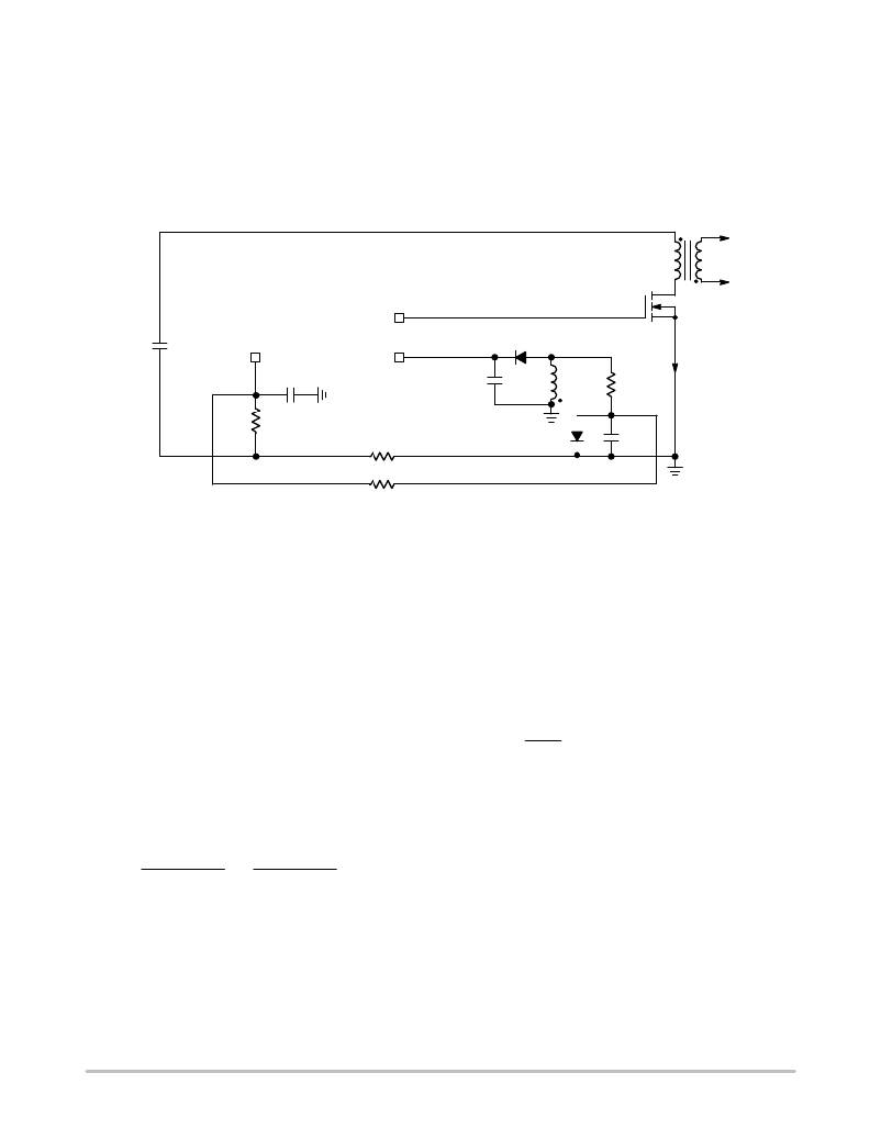
�NCP1351�
�Over� power� protection� can� be� done� without� power�
�dissipation� penalty� by� arranging� components� around� the�
�auxiliary� as� suggested� by� Figure� 14.� On� this� schematic,� the�
�diode� anode� swings� negative� during� the� on� time.� This�
�negative� level� directly� depends� on� the� input� voltage� and�
�offsets� the� current� sense� pin� via� the� R� OPP� resistor.� A� small�
�integration� is� necessary� to� reduce� the� O� PP� action� in� light� load�
�the� standby� power� can� be� affected.� Again,� the� resistor� R� OPP�
�should� be� placed� as� close� as� possible� to� the� CS� pin.� The�
�22� pF� can� help� to� circumvent� any� picked-up� noise� and� D� 2�
�prevents� the� positive� loading� of� the� 270� pF� capacitor� during�
�the� flyback� swing.� We� have� put� a� typical� 100� k� W� O� PP�
�resistor� but� a� tweak� is� required� depending� on� your�
�application.�
�conditions.� However,� depending� on� the� compensation� level,�
�L� P�
�DRV�
�DRV�
�+�
�CS�
�V� CC�
�D� aux�
�C� Bulk�
�C4�
�22p�
�+�
�CV� CC�
�L� aux�
�R1�
�I� Lp�
�150k�
�R� offset�
�R� sense�
�D2�
�1N4148�
�C3�
�270p�
�R� OPP�
�100k�
�Figure� 14.� The� OPP� is� Relatively� Easy� to� Implement� and� It� Does� not� Waste� Power�
�Suppose� you� would� need� to� reduce� the� peak� current� by�
�15%� in� high-line� conditions.� The� turn-ratio� between� the�
�auxiliary� winding� and� the� primary� winding� is� N� aux� .� Assume�
�its� value� is� 0.15.� Thus,� the� voltage� on� D� aux� cathode� swings�
�Typically,� we� measured� around� –4� V� on� our� 50� W� prototype.�
�By� calculation,� we� want� to� decrease� the� peak� current� by�
�15%.� Compared� to� the� internal� 270� m� A� source,� we� need� to�
�derive:�
�negative� during� the� on� time� to� a� level� of:�
�Vaux_peak� +� -Vin_max� Naux� +� -375�
�0.15� +� -56� V�
�Ioffset� +� -0.15�
�270� m� +� -40.5� m� A�
�(eq.� 11)�
�(eq.� 8)�
�Thus,� from� the� –4� V� excursion,� the� R� OPP� resistor� is�
�If� we� selected� a� 3.7� k� W� resistor� for� R� offset� ,� then� the�
�maximum� sense� voltage� being� developed� is:�
�Vsense� +� 3.7� k� 270� m� +� 1� V� (eq.� 9)�
�derived� by:�
�ROPP� +�
�4�
�40.5� m�
�+� 98� k� W�
�(eq.� 12)�
�The� small� RC� network� made� of� R� 1� and� C� 3� ,� purposely� limits�
�the� voltage� excursion� on� D� 2� anode.� Assume� the� primary�
�inductance� value� gives� an� on� time� of� 3� m� s� at� high-line.� The�
�voltage� across� C� 3� thus� swings� down� to:�
�After� experimental� measurements,� the� resistor� was�
�normalized� down� to� 100� k� W� .�
�Feedback�
�Unlike� other� controllers,� the� feedback� in� the� NCP1351�
�VC3� +�
�tonVaux_peak�
�R1C3�
�+� -�
�3� m�
�150� k�
�56�
�270� p�
�+� -4.2� V�
�(eq.�
�10)�
�works� in� current� rather� than� voltage.� Figure� 15� details� the�
�internal� circuitry� of� this� particular� section.� The� optocoupler�
�injects� a� current� into� the� FB� pin� in� relationship� with� the�
�input/output� conditions.�
�http://onsemi.com�
�13�
�相关PDF资料 |
PDF描述 |
|---|---|
| TAP685K035HSC | CAP TANT 6.8UF 35V 10% RADIAL |
| TAP685K035HCD | CAP TANT 6.8UF 35V 10% RADIAL |
| LC4384C-5FTN256I | IC CPLD 384MACROCELLS 256FTBGA |
| RS-1215S/H3 | CONV DC/DC 2W 9-18VIN 15VOUT |
| VE-BT0-CY-F4 | CONVERTER MOD DC/DC 5V 50W |
相关代理商/技术参数 |
参数描述 |
|---|---|
| NCP1351CDR2G | 功能描述:电流型 PWM 控制器 PWM CONTROLLER RoHS:否 制造商:Texas Instruments 开关频率:27 KHz 上升时间: 下降时间: 工作电源电压:6 V to 15 V 工作电源电流:1.5 mA 输出端数量:1 最大工作温度:+ 105 C 安装风格:SMD/SMT 封装 / 箱体:TSSOP-14 |
| NCP1351CPG | 功能描述:电流型 PWM 控制器 VRIABLE OFF TM CNTRL RoHS:否 制造商:Texas Instruments 开关频率:27 KHz 上升时间: 下降时间: 工作电源电压:6 V to 15 V 工作电源电流:1.5 mA 输出端数量:1 最大工作温度:+ 105 C 安装风格:SMD/SMT 封装 / 箱体:TSSOP-14 |
| NCP1351DDR2G | 功能描述:电流型 PWM 控制器 PWM CONTROLLER RoHS:否 制造商:Texas Instruments 开关频率:27 KHz 上升时间: 下降时间: 工作电源电压:6 V to 15 V 工作电源电流:1.5 mA 输出端数量:1 最大工作温度:+ 105 C 安装风格:SMD/SMT 封装 / 箱体:TSSOP-14 |
| NCP1351DPG | 功能描述:电流型 PWM 控制器 VRIABLE OFF TM CNTRL RoHS:否 制造商:Texas Instruments 开关频率:27 KHz 上升时间: 下降时间: 工作电源电压:6 V to 15 V 工作电源电流:1.5 mA 输出端数量:1 最大工作温度:+ 105 C 安装风格:SMD/SMT 封装 / 箱体:TSSOP-14 |
| NCP1351LEDGEVB | 功能描述:电源管理IC开发工具 20 W CONSTANT CUR LED DRV RoHS:否 制造商:Maxim Integrated 产品:Evaluation Kits 类型:Battery Management 工具用于评估:MAX17710GB 输入电压: 输出电压:1.8 V |
发布紧急采购,3分钟左右您将得到回复。