- 您现在的位置:买卖IC网 > PDF目录19516 > NCP1382DR2G (ON Semiconductor)IC CTRLR PWM OVP OTP 14SOIC PDF资料下载
参数资料
| 型号: | NCP1382DR2G |
| 厂商: | ON Semiconductor |
| 文件页数: | 12/25页 |
| 文件大小: | 0K |
| 描述: | IC CTRLR PWM OVP OTP 14SOIC |
| 标准包装: | 2,500 |
| 输出隔离: | 隔离 |
| 频率范围: | 调节 |
| 输入电压: | 9 V ~ 20 V |
| 工作温度: | 0°C ~ 125°C |
| 封装/外壳: | 14-SOIC(0.154",3.90mm 宽) |
| 供应商设备封装: | 14-SOICN |
| 包装: | 带卷 (TR) |
�� �
�
�NCP1381,� NCP1382�
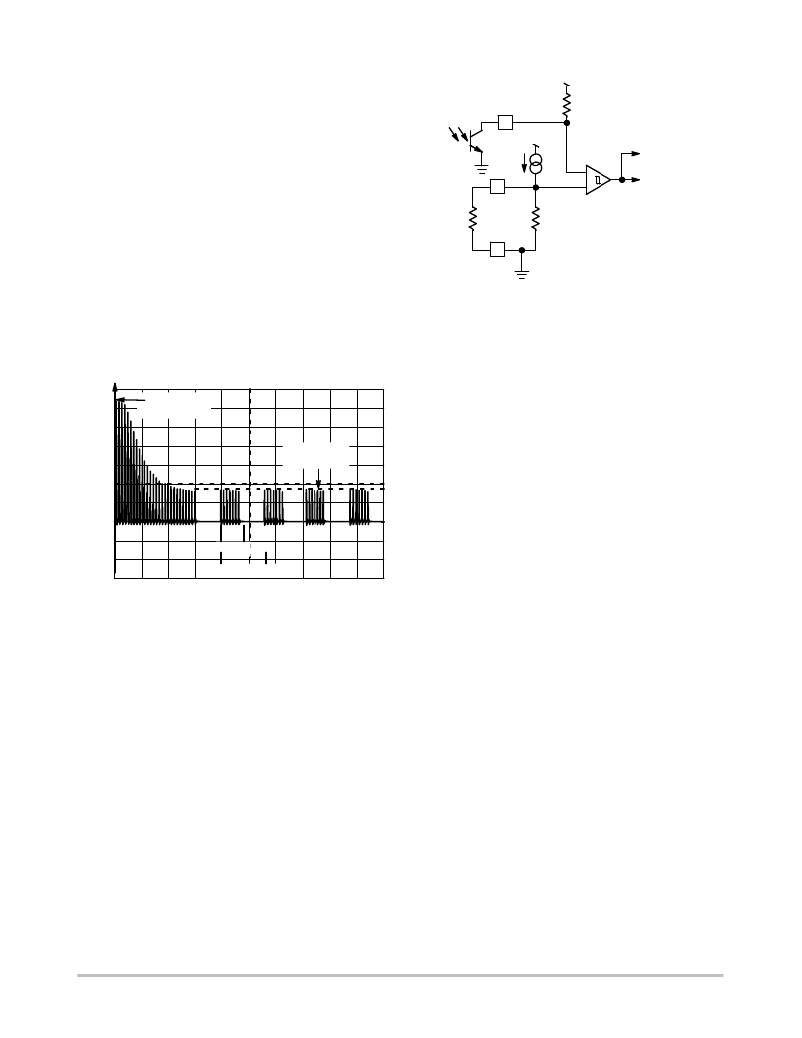
�Figure� 12� depicts� the� internal� comparator� arrangement.�
�The� FB� pin� level� is� permanently� compared� to� a� fixed� level,�
�V� DD�
�V� skip�
�Reset�
�V� skip� ,� also� available� on� Pin� 5� for� adjustment.� As� a� result,� the�
�user� can� wire� a� resistor� to� ground� and� alter� the� skip� level� in�
�case� of� noise� problems.� When� the� FB� pin� is� above� V� skip� ,� the�
�comparator� is� transparent� to� the� operation.� When� the� load�
�becomes� lighter,� the� FB� level� goes� down� too.� When� it�
�reaches� V� skip� ,� the� comparator� goes� high� and� resets� the�
�internal� flip--flop:� the� driving� pulses� are� stopped.� As� a� result,�
�V� out� starts� to� also� decrease� since� no� energy� transfer� is�
�ensured.� Detecting� a� decay� in� the� output� voltage,� the� FB� loop�
�will� react� by� increasing� its� level.� When� the� level� crosses�
�R�
�6�
�30� m� A�
�5�
�25� k�
�8�
�V� DD�
�Soft--Start�
�Activation�
�--�
�+�
�Hysteresis� =� 50� mV�
�V� skip� plus� a� slight� hysteresis,� pulses� restart� again:� a� ripple�
�occurs� on� the� FB� pin.� Please� note� that� the� soft--start� will� be�
�activated� every� time� the� skip� comparator� asks� to� restart.�
�Therefore,� instead� of� having� sharp� skip� transitions,� a� smooth�
�current� rampup� can� be� observed� on� the� current� envelope.�
�This� option� significantly� decreases� the� acoustical� noise.�
�Figure� 13� shows� a� typical� shot� and� Figure� 15� portrays�
�several� skip� cycles.�
�Maximum�
�Peak� Current�
�200�
�Skip� Cycle�
�Current� Limit�
�100�
�0�
�Width�
�Recurrence�
�Figure� 11.� The� Skip� Cycle� Takes� Place� at� Low� Peak�
�Currents� Which� Guaranties� Noise� Free� Operation�
�Figure� 12.� A� Resistor� to� GND� can� Adjust� the� Skip�
�Level�
�As� soon� as� the� feedback� voltage� goes� up� again,� there� can�
�be� two� situations� as� we� have� seen� before:� in� normal�
�operating� conditions,� e.g.� when� the� drain� oscillations� are�
�generous,� the� demagnetization� comparator� can� detect� the�
�45� mV� crossing� and� gives� the� “green� light”,� alone,� to�
�reactive� the� power� switch.� However,� when� skip� cycle� takes�
�place� (e.g.� at� low� output� power� demands),� the� restart� event�
�slides� along� the� drain� ringing� waveforms� (actually� the� valley�
�locations)� which� decays� more� or� less� quickly,� depending� on�
�the� L� primary� --C� parasitic� network� damping� factor.� The� situation�
�can� thus� quickly� occur� where� the� ringing� becomes� too� weak�
�to� be� detected� by� the� demagnetization� comparator:� it� then�
�permanently� stays� locked� in� a� given� position� and� can� no�
�longer� deliver� the� “green� light”� to� the� controller.� To� help� in�
�this� situation,� the� NCP1381/82� implements� a� 8� m� s� timeout�
�generator:� each� time� the� 45� mV� crossing� occurs,� the� timeout�
�is� reset.� So,� as� long� as� the� ringing� becomes� too� low,� the�
�timeout� generator� starts� to� count� and� after� 8� m� s,� it� delivers� its�
�“green� light”.� If� the� skip� signal� is� already� present� then� the�
�controller� restarts;� otherwise� the� logic� waits� for� it� to� release�
�the� reset� input� and� set� the� drive� output� high.� Figure� 14�
�depicts� these� two� different� situations:�
�http://onsemi.com�
�12�
�相关PDF资料 |
PDF描述 |
|---|---|
| VI-B0N-CY-F3 | CONVERTER MOD DC/DC 18.5V 50W |
| R15P215S/X2/P/R6.4 | CONV DC/DC 2W 15VIN 15VOUT |
| V24A12E400B3 | CONVERTER MOD DC/DC 12V 400W |
| RCB105DHNT | CONN EDGECARD 210PS DIP .050 SLD |
| TPSR475M010R3000 | CAP TANT 4.7UF 10V 20% 0805 |
相关代理商/技术参数 |
参数描述 |
|---|---|
| NCP1392B | 制造商:ONSEMI 制造商全称:ON Semiconductor 功能描述:High-Voltage Half-Bridge Driver with Inbuilt Oscillator |
| NCP1392B_09 | 制造商:ONSEMI 制造商全称:ON Semiconductor 功能描述:High-Voltage Half-Bridge Driver with Inbuiltc Oscillator |
| NCP1392BDR2G | 功能描述:功率驱动器IC HV HALF-BRIDGE DRVER RoHS:否 制造商:Micrel 产品:MOSFET Gate Drivers 类型:Low Cost High or Low Side MOSFET Driver 上升时间: 下降时间: 电源电压-最大:30 V 电源电压-最小:2.75 V 电源电流: 最大功率耗散: 最大工作温度:+ 85 C 安装风格:SMD/SMT 封装 / 箱体:SOIC-8 封装:Tube |
| NCP1392DDR2G | 功能描述:功率驱动器IC HV HALF-BRIDGE DRIVER RoHS:否 制造商:Micrel 产品:MOSFET Gate Drivers 类型:Low Cost High or Low Side MOSFET Driver 上升时间: 下降时间: 电源电压-最大:30 V 电源电压-最小:2.75 V 电源电流: 最大功率耗散: 最大工作温度:+ 85 C 安装风格:SMD/SMT 封装 / 箱体:SOIC-8 封装:Tube |
| NCP1392LCDTVGEVB | 功能描述:BOARD EVAL NCP1392HV RoHS:是 类别:编程器,开发系统 >> 评估板 - DC/DC 与 AC/DC(离线)SMPS 系列:* 产品培训模块:Obsolescence Mitigation Program 标准包装:1 系列:True Shutdown™ 主要目的:DC/DC,步升 输出及类型:1,非隔离 功率 - 输出:- 输出电压:- 电流 - 输出:1A 输入电压:2.5 V ~ 5.5 V 稳压器拓扑结构:升压 频率 - 开关:3MHz 板类型:完全填充 已供物品:板 已用 IC / 零件:MAX8969 |
发布紧急采购,3分钟左右您将得到回复。