- 您现在的位置:买卖IC网 > PDF目录13758 > NCP1523BFCT2G (ON Semiconductor)IC REG BUCK SYNC ADJ 8FLIPCHIP PDF资料下载
参数资料
| 型号: | NCP1523BFCT2G |
| 厂商: | ON Semiconductor |
| 文件页数: | 14/16页 |
| 文件大小: | 0K |
| 描述: | IC REG BUCK SYNC ADJ 8FLIPCHIP |
| 标准包装: | 3,000 |
| 类型: | 降压(降压) |
| 输出类型: | 可调式 |
| 输出数: | 1 |
| 输出电压: | 0.9 V ~ 3.3 V |
| 输入电压: | 2.7 V ~ 5.5 V |
| PWM 型: | 电压模式 |
| 频率 - 开关: | 3MHz |
| 电流 - 输出: | 600mA |
| 同步整流器: | 是 |
| 工作温度: | -40°C ~ 85°C |
| 安装类型: | 表面贴装 |
| 封装/外壳: | 8-WFBGA,FCBGA |
| 包装: | 带卷 (TR) |
| 供应商设备封装: | 8-覆晶 |
�� �
�
�NCP1523�
�APPLICATION� INFORMATION�
�Output� Voltage� Selection�
�The� output� voltage� is� programmed� through� an� external�
�resistor� divider� connected� from� ADJ� to� FB� then� to� GND.� For�
�low� power� consumption� and� noise� immunity,� the� resistor�
�from� FB� to� GND� (R2)� should� be� in� the� [100� k� W� ?� 600� k� W� ]�
�range.� If� R2� is� 200� k� W� given� the� V� FB� is� 0.6� V,� the� current�
�through� the� divider� will� be� 3� m� A.�
�The� formula� below� gives� the� value� of� V� OUT� ,� given� the�
�desired� R1� and� the� R1� value,�
�The� device� operates� with� inductance� value� between� 1� m� H�
�and� maximum� of� 4.7� m� H.�
�If� the� corner� frequency� is� moved,� it� is� recommended� to�
�check� the� loop� stability� depending� of� the� output� ripple�
�voltage� accepted� and� output� current� required.� For� lower�
�frequency,� the� stability� will� be� increase;� a� larger� output�
�capacitor� value� could� be� chosen� without� critical� effect� on� the�
�system.� On� the� other� hand,� a� smaller� capacitor� value�
�increases� the� corner� frequency� and� it� should� be� critical� for�
�1� )� R1�
�VOUT� +� VFB�
�R2�
�the� system� stability.� Take� care� to� check� the� loop� stability.�
�The� phase� margin� is� usually� higher� than� 45� °� .�
�?�
�?�
�?�
�?�
�V� OUT� :� output� voltage� (volts)�
�V� FB� :� feedback� voltage� =� 0.6� V�
�R1:� feedback� resistor� from� V� OUT� to� FB�
�R2:� feedback� resistor� from� FB� to� GND�
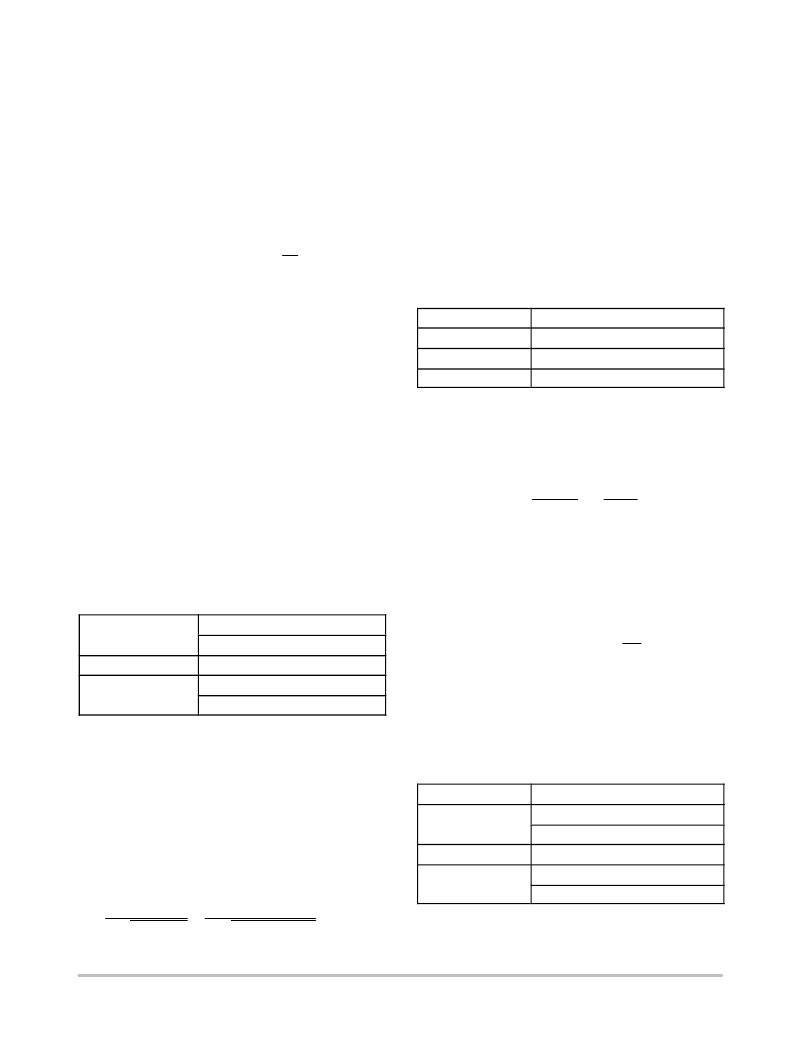
�Table� 2.� L?C� FILTER� EXAMPLE�
�Inductance� (L)� Output� Capacitor� (C� OUT� )�
�1� m� H� 10� m� F�
�Input� Capacitor� Selection�
�In� PWM� operating� mode,� the� input� current� is� pulsating�
�with� large� switching� noise.� Using� an� input� bypass� capacitor�
�2.2� m� H�
�4.7� m� H�
�4.7� m� F�
�2.2� m� F�
�1?� OUT�
�D� IL� +�
�can� reduce� the� peak� current� transients� drawn� from� the� input�
�supply� source,� thereby� reducing� switching� noise�
�significantly.� The� capacitance� needed� for� the� input� bypass�
�capacitor� depends� on� the� source� impedance� of� the� input�
�supply.�
�The� maximum� RMS� current� occurs� at� 50%� duty� cycle�
�with� maximum� output� current,� which� is� IO,� max/2.�
�For� NCP1523,� a� low� profile� ceramic� capacitor� of� 4.7� m� F�
�should� be� used� for� most� of� the� cases.� For� effective� bypass�
�results,� the� input� capacitor� should� be� placed� as� close� as�
�possible� to� the� V� IN� Pin.�
�Table� 1.� LIST� OF� INPUT� CAPACITOR�
�Inductor� Selection�
�The� inductor� parameters� directly� related� to� device�
�performances� are� saturation� current� and� DC� resistance� and�
�inductance� value.� The� inductor� ripple� current� (� D� I� L� )�
�decreases� with� higher� inductance:�
�VOUT� V�
�L� fSW� VIN�
�D� I� L� =� peak� to� peak� inductor� ripple� current�
�L� =� inductor� value�
�f� SW� =� Switching� frequency�
�The� Saturation� current� of� the� inductor� should� be� rated�
�higher� than� the� maximum� load� current� plus� half� the� ripple�
�Murata�
�GRM188R60J475KE�
�GRM21BR71C475KA�
�current:�
�IL(MAX)� +� IO(MAX)� )�
�D� IL�
�2�
�Taiyo� Yuden�
�TDK�
�JMK212BY475MG�
�C2012X5R0J475KT�
�C1608X5R0J475KT�
�I� L(MAX)� Maximum� inductor� current�
�I� O(MAX)� Maximum� Output� current�
�The� inductor� ’s� resistance� will� factor� into� the� overall�
�efficiency� of� the� converter.� For� best� performances,� the� DC�
�Output� L?C� Filter� Design� Considerations:�
�The� NCP1523� is� built� in� 3� MHz� frequency� and� uses�
�voltage� mode� architecture.� The� correct� selection� of� the�
�output� filter� ensures� good� stability� and� fast� transient�
�resistance� should� be� less� than� 0.3� W� for� good� efficiency.�
�Table� 3.� LIST� OF� INDUCTOR�
�response.�
�Due� to� the� nature� of� the� buck� converter,� the� output� L?C�
�filter� must� be� selected� to� work� with� internal� compensation.�
�For� NCP1523,� the� internal� compensation� is� internally� fixed�
�and� it� is� optimized� for� an� output� filter� of� L� =� 2.2� m� H� and�
�C� OUT� =� 4.7� m� F�
�The� corner� frequency� is� given� by:�
�FDK�
�TDK�
�Taiyo� Yuden�
�Coil� Craft�
�MIPW3226� Series�
�VLF3010AT� Series�
�TFC252005� Series�
�LQ� CBL2012�
�DO1605?T� Series�
�LPO3010�
�fc� +�
�2� p� L�
�1�
�COUT�
�+�
�1�
�2� p� 2.2� m� H�
�4.7� m� F�
�+� 49.5� KHz�
�http://onsemi.com�
�14�
�相关PDF资料 |
PDF描述 |
|---|---|
| UWT1H0R1MCL2GB | CAP ALUM 0.1UF 50V 20% SMD |
| RMM12DRSI | CONN EDGECARD 24POS DIP .156 SLD |
| RBM24DCSI | CONN EDGECARD 48POS DIP .156 SLD |
| GCA35DCBI | CONN EDGECARD 70POS R/A .125 SLD |
| ECA32DCBI | CONN EDGECARD 64POS R/A .125 SLD |
相关代理商/技术参数 |
参数描述 |
|---|---|
| NCP1523BGEVB | 功能描述:电源管理IC开发工具 NCP1523B EVAL BRD RoHS:否 制造商:Maxim Integrated 产品:Evaluation Kits 类型:Battery Management 工具用于评估:MAX17710GB 输入电压: 输出电压:1.8 V |
| NCP1523FCT2G | 功能描述:直流/直流开关转换器 UBUMP DCDC RoHS:否 制造商:STMicroelectronics 最大输入电压:4.5 V 开关频率:1.5 MHz 输出电压:4.6 V 输出电流:250 mA 输出端数量:2 最大工作温度:+ 85 C 安装风格:SMD/SMT |
| NCP1526EVB | 功能描述:电源管理IC开发工具 NCP1526 EVALUATION BOARD RoHS:否 制造商:Maxim Integrated 产品:Evaluation Kits 类型:Battery Management 工具用于评估:MAX17710GB 输入电压: 输出电压:1.8 V |
| NCP1526MUTXG | 功能描述:直流/直流开关转换器 BUCK REG AND LDO RoHS:否 制造商:STMicroelectronics 最大输入电压:4.5 V 开关频率:1.5 MHz 输出电压:4.6 V 输出电流:250 mA 输出端数量:2 最大工作温度:+ 85 C 安装风格:SMD/SMT |
| NCP1529ASNT1G | 功能描述:直流/直流开关转换器 STEP-DOWN CONVERTER RoHS:否 制造商:STMicroelectronics 最大输入电压:4.5 V 开关频率:1.5 MHz 输出电压:4.6 V 输出电流:250 mA 输出端数量:2 最大工作温度:+ 85 C 安装风格:SMD/SMT |
发布紧急采购,3分钟左右您将得到回复。