- 您现在的位置:买卖IC网 > PDF目录13758 > NCP1523BFCT2G (ON Semiconductor)IC REG BUCK SYNC ADJ 8FLIPCHIP PDF资料下载
参数资料
| 型号: | NCP1523BFCT2G |
| 厂商: | ON Semiconductor |
| 文件页数: | 3/16页 |
| 文件大小: | 0K |
| 描述: | IC REG BUCK SYNC ADJ 8FLIPCHIP |
| 标准包装: | 3,000 |
| 类型: | 降压(降压) |
| 输出类型: | 可调式 |
| 输出数: | 1 |
| 输出电压: | 0.9 V ~ 3.3 V |
| 输入电压: | 2.7 V ~ 5.5 V |
| PWM 型: | 电压模式 |
| 频率 - 开关: | 3MHz |
| 电流 - 输出: | 600mA |
| 同步整流器: | 是 |
| 工作温度: | -40°C ~ 85°C |
| 安装类型: | 表面贴装 |
| 封装/外壳: | 8-WFBGA,FCBGA |
| 包装: | 带卷 (TR) |
| 供应商设备封装: | 8-覆晶 |
�� �
�
�NCP1523�
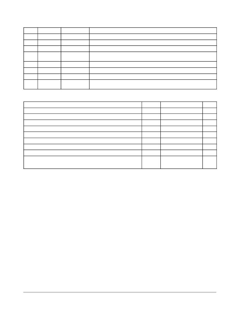
�PIN� FUNCTION� DESCRIPTION�
�Pin�
�A1�
�A2�
�B1�
�B2�
�Pin� Name�
�GND�
�V� IN�
�S� W�
�EN�
�Type�
�Power� Ground�
�Power� Input�
�Analog� Output�
�Digital� Input�
�Description�
�Ground� connection� for� the� NFET� Power� Stage� and� the� analog� sections.�
�Power� Supply� Input� for� the� PFET� Power� Stage� and� the� Analog� Sections� of� the� IC.�
�Connection� from� Power� MOSFETs� to� the� Inductor.�
�Enable� for� Switching� Regulator.� This� pin� is� active� high.� This� pin� contains� an� internal�
�pulldown� resistor.�
�C1�
�C2�
�D1�
�D2�
�GND�
�ADJ�
�V� OUT�
�FB�
�Power� Ground�
�Analog� Input�
�Analog� Input�
�Analog� Input�
�Ground� connection� for� the� NFET� Power� Stage� and� the� analog� sections.�
�This� pin� is� the� compensation� input.� R1� is� connected� to� this� pin.�
�This� pin� is� connected� of� the� converter� ’s� output.� This� is� the� sense� of� the� output� voltage.�
�Feedback� voltage� from� the� output� of� the� power� supply.� This� is� the� input� to� the� error�
�amplifier.�
�MAXIMUM� RATINGS�
�Rating�
�Minimum� Voltage� All� Pins�
�Maximum� Voltage� All� Pins� (Note� 1)�
�Maximum� Voltage� Enable,� FB,� SW�
�Thermal� Resistance,� Junction?to?Air� (Note� 2)�
�Operating� Ambient� Temperature� Range�
�Storage� Temperature� Range�
�Junction� Operating� Temperature�
�Latch?up� Current� Maximum� Rating� T� A� =� 85� °� C� (Note� 4)�
�ESD� Withstand� Voltage� (Note� 3)�
�Human� Body� Model�
�Machine� Model�
�Symbol�
�V� MIN�
�V� MAX�
�V� MAX�
�R� q� JA�
�T� A�
�T� STG�
�T� J�
�L� U�
�V� ESD�
�Value�
�?0.3�
�7�
�V� IN� +� 0.3�
�159�
�?40� to� 85�
�?55� to� 150�
�?40� to� 125�
�"� 100�
�2.0�
�200�
�Unit�
�V�
�V�
�V�
�°� C/W�
�°� C�
�°� C�
�°� C�
�mA�
�kV�
�V�
�Stresses� exceeding� Maximum� Ratings� may� damage� the� device.� Maximum� Ratings� are� stress� ratings� only.� Functional� operation� above� the�
�Recommended� Operating� Conditions� is� not� implied.� Extended� exposure� to� stresses� above� the� Recommended� Operating� Conditions� may� affect�
�device� reliability.�
�1.� According� to� JEDEC� standard� JESD22?A108B�
�2.� For� the� 8?Pin� Chip� Scale� Package,� the� R� q� JA� is� highly� dependent� of� the� PCB� heatsink� area.� R� q� JA� =� 159� °� C/W� with� 50� mm� 2� PCB� heatsink� area.�
�3.� This� device� series� contains� ESD� protection� and� exceeds� the� following� tests:�
�Human� Body� Model� (HBM)� $� 2.0� kV� per� JEDEC� standard:� JESD22?A114�
�Machine� Model� (MM)� $� 200� V� per� JEDEC� standard:� JESD22?A115�
�4.� Latchup� current� maximum� rating� per� JEDEC� standard:� JESD78.�
�http://onsemi.com�
�3�
�相关PDF资料 |
PDF描述 |
|---|---|
| UWT1H0R1MCL2GB | CAP ALUM 0.1UF 50V 20% SMD |
| RMM12DRSI | CONN EDGECARD 24POS DIP .156 SLD |
| RBM24DCSI | CONN EDGECARD 48POS DIP .156 SLD |
| GCA35DCBI | CONN EDGECARD 70POS R/A .125 SLD |
| ECA32DCBI | CONN EDGECARD 64POS R/A .125 SLD |
相关代理商/技术参数 |
参数描述 |
|---|---|
| NCP1523BGEVB | 功能描述:电源管理IC开发工具 NCP1523B EVAL BRD RoHS:否 制造商:Maxim Integrated 产品:Evaluation Kits 类型:Battery Management 工具用于评估:MAX17710GB 输入电压: 输出电压:1.8 V |
| NCP1523FCT2G | 功能描述:直流/直流开关转换器 UBUMP DCDC RoHS:否 制造商:STMicroelectronics 最大输入电压:4.5 V 开关频率:1.5 MHz 输出电压:4.6 V 输出电流:250 mA 输出端数量:2 最大工作温度:+ 85 C 安装风格:SMD/SMT |
| NCP1526EVB | 功能描述:电源管理IC开发工具 NCP1526 EVALUATION BOARD RoHS:否 制造商:Maxim Integrated 产品:Evaluation Kits 类型:Battery Management 工具用于评估:MAX17710GB 输入电压: 输出电压:1.8 V |
| NCP1526MUTXG | 功能描述:直流/直流开关转换器 BUCK REG AND LDO RoHS:否 制造商:STMicroelectronics 最大输入电压:4.5 V 开关频率:1.5 MHz 输出电压:4.6 V 输出电流:250 mA 输出端数量:2 最大工作温度:+ 85 C 安装风格:SMD/SMT |
| NCP1529ASNT1G | 功能描述:直流/直流开关转换器 STEP-DOWN CONVERTER RoHS:否 制造商:STMicroelectronics 最大输入电压:4.5 V 开关频率:1.5 MHz 输出电压:4.6 V 输出电流:250 mA 输出端数量:2 最大工作温度:+ 85 C 安装风格:SMD/SMT |
发布紧急采购,3分钟左右您将得到回复。