- 您现在的位置:买卖IC网 > PDF目录22197 > NCP1606BPG (ON Semiconductor)IC CTRLR PWR FACTOR 0.5V 8-DIP PDF资料下载
参数资料
| 型号: | NCP1606BPG |
| 厂商: | ON Semiconductor |
| 文件页数: | 11/22页 |
| 文件大小: | 245K |
| 描述: | IC CTRLR PWR FACTOR 0.5V 8-DIP |
| 产品变化通告: | Product Obsolescence 05/Oct/2010 |
| 标准包装: | 50 |
| 模式: | 临界传导(CRM) |
| 电流 - 启动: | 20µA |
| 电源电压: | 10.3 V ~ 20 V |
| 工作温度: | -40°C ~ 125°C |
| 安装类型: | 通孔 |
| 封装/外壳: | 8-DIP(0.300",7.62mm) |
| 供应商设备封装: | 8-PDIP |
| 包装: | 管件 |
NCP1606
http://onsemi.com
11
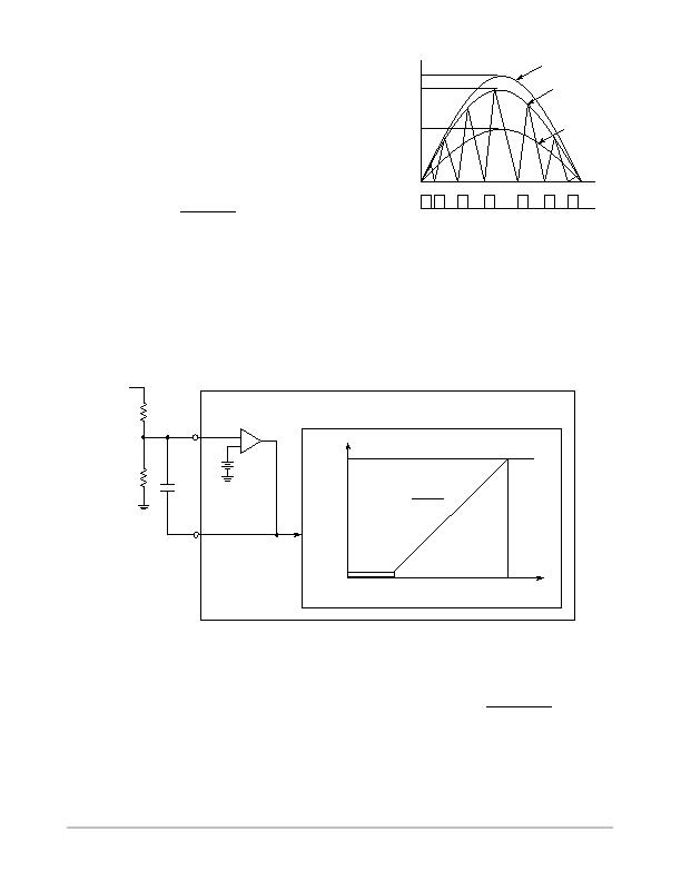
When the switch is closed, the inductor current increases
linearly to its peak value. When the switch opens, the
inductor current linearly decreases to zero. At this point,
the drain voltage of the switch (V
d
) is essentially floating
and begins to drop. If the next switching cycle does not
start, then the voltage will ring with a dampened frequency
around V
in
. A simple derivation of equations (such as found
in AND8123), leads to the result that good power factor
correction in CRM operation is achieved when the on time
is constant across an ac cycle and is equal to:
t
on
+
2 @ P
OUT
@ L
h @ Vac
RMS
2
(eq. 1)
A simple plot of this switching over an ac line cycle is
illustrated in Figure 24. The off time varies based on the
instantaneous line voltage, but the on time is kept constant.
This naturally causes the peak inductor current (I
Lpk
) to
follow the ac line voltage.
The NCP1606 represents an ideal method to implement
this constant on time CRM control in a cost effective and
robust solution. The device incorporates an accurate
regulation circuit, a low power startup circuit, and
advanced protection features.
Figure 24. Inductor Waveform During CRM Operation
ON
OFF
MOSFET
I
in
(t)
I
L
(t)
V
in
(t)
V
inpk
I
Lpk
I
inpk
ERROR AMPLIFIER REGULATION
The NCP1606 is configured to regulate the boost output
voltage based on its built in error amplifier (EA). The error
amplifiers negative terminal is pinned out to FB, the
positive terminal is tied to a 2.5 V ?1.6% reference, and the
output is pinned out to Control (Figure 25).
Figure 25. Error Amplifier and On Time Regulation Circuits
FB
Control
+
EA
2.5 V
PWM BLOCK
V
CONTROL
R
OUT2
R
OUT1
C
COMP
t
PWM
t
ON(max)
V
OUT
t
ON
V
EAL
V
EAH
Slope +
Ct
I
CHARGE
V
CONTROL
A resistor divider from the boost output to the input of the
EA sets the FB level. If the output voltage is too low, then
the FB level will drop and the EA will cause the control
voltage to increase. This increases the on time of the driver,
which increases the power delivered and brings the output
back into regulation. Alternatively, if the output voltage
(and hence FB voltage) is too high, then the control level
decreases and the driver on times are shortened. In this way,
the circuit regulates the output voltage (V
OUT
) so that the
V
OUT
portion that is applied to FB through the resistor
divider R
OUT1
and R
OUT2
is equal to the internal reference
(2.5 V). The output voltage can then be easily set according
to the following equation:
V
OUT
+ 2.5 V @
R
OUT1
) R
OUT2
R
OUT2
(eq. 2)
A compensation network is placed between the FB and
Control pins to reduce the speed at which the EA responds
to changes in the boost output. This is necessary due to the
nature of an active PFC circuit. The PFC stage absorbs a
sinusoidal current from a sinusoidal line voltage. Hence,
the converter provides the load with a power that matches
相关PDF资料 |
PDF描述 |
|---|---|
| RCM10DRYH | CONN EDGECARD 20POS DIP .156 SLD |
| RAC10-12SA-E | CONV AC/DC 90-264VAC 12V 833MA |
| NCP1606APG | IC CTRLR PWR FACTOR 1.7V 8-DIP |
| RAC10-05SA-E | CONV AC/DC 90-264VAC 5V 2A |
| RCM12DRXN | CONN EDGECARD 24POS DIP .156 SLD |
相关代理商/技术参数 |
参数描述 |
|---|---|
| NCP1607BDR2G | 功能描述:功率因数校正 IC CST EFCT PW FCTR CTR RoHS:否 制造商:Fairchild Semiconductor 开关频率:300 KHz 最大功率耗散: 最大工作温度:+ 125 C 安装风格:SMD/SMT 封装 / 箱体:SOIC-8 封装:Reel |
| NCP1607BOOSTGEVB | 功能描述:BOARD EVAL NCP1607 100W BOOST RoHS:是 类别:编程器,开发系统 >> 评估演示板和套件 系列:* 标准包装:1 系列:PCI Express® (PCIe) 主要目的:接口,收发器,PCI Express 嵌入式:- 已用 IC / 零件:DS80PCI800 主要属性:- 次要属性:- 已供物品:板 |
| NCP1608BDR2G | 功能描述:功率因数校正 IC COST EFFECT PWR FACT CONT RoHS:否 制造商:Fairchild Semiconductor 开关频率:300 KHz 最大功率耗散: 最大工作温度:+ 125 C 安装风格:SMD/SMT 封装 / 箱体:SOIC-8 封装:Reel |
| NCP1608BOOSTGEVB | 功能描述:电源管理IC开发工具 NCP1608 100 W BOOST EVB PWR SPY RoHS:否 制造商:Maxim Integrated 产品:Evaluation Kits 类型:Battery Management 工具用于评估:MAX17710GB 输入电压: 输出电压:1.8 V |
| NCP1611ADR2G | 功能描述:功率因数校正 IC NCP1611A ENHANCED PFC RoHS:否 制造商:Fairchild Semiconductor 开关频率:300 KHz 最大功率耗散: 最大工作温度:+ 125 C 安装风格:SMD/SMT 封装 / 箱体:SOIC-8 封装:Reel |
发布紧急采购,3分钟左右您将得到回复。