- 您现在的位置:买卖IC网 > Datasheet目录45 > NCP1611BDR2G (ON Semiconductor)IC PFC CTLR HE ENHANCED 8-SOIC Datasheet资料下载
参数资料
| 型号: | NCP1611BDR2G |
| 厂商: | ON Semiconductor |
| 文件页数: | 4/29页 |
| 文件大小: | 879K |
| 描述: | IC PFC CTLR HE ENHANCED 8-SOIC |
| 标准包装: | 3,000 |
| 系列: | * |
第1页第2页第3页当前第4页第5页第6页第7页第8页第9页第10页第11页第12页第13页第14页第15页第16页第17页第18页第19页第20页第21页第22页第23页第24页第25页第26页第27页第28页第29页
NCP1611
http://onsemi.com
4
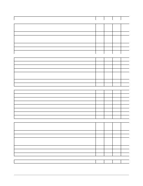
TYPICAL ELECTRICAL CHARACTERISTICS (Conditions: V
CC
= 15 V, T
J
from 40癈 to +125癈, unless otherwise specified)
Symbol
Rating
Min
Typ
Max
Unit
STARTUP AND SUPPLY CIRCUIT
V
CC(on)
StartUp Threshold, V
CC
increasing:
A version
B version
9.75
15.80
10.50
17.00
11.25
18.20
V
V
CC(off)
Minimum Operating Voltage, V
CC
falling
8.50
9.00
9.50
V
V
CC(HYST)
Hysteresis (V
CC(on)
V
CC(off)
)
A version
B version
0.75
6.00
1.50
8.00
V
I
CC(start)
StartUp Current, V
CC
= 9.4 V
20
50
mA
I
CC(op)1
Operating Consumption, no switching (V
sense
pin being grounded)
0.5
1.0
mA
I
CC(op)2
Operating Consumption, 50 kHz switching, no load on DRV pin
2.0
3.0
mA
CURRENT CONTROLLED FREQUENCY FOLDBACK
T
DT1
DeadTime, V
FFcontrol
= 2.60 V (Note 6)
0
ms
T
DT2
DeadTime, V
FFcontrol
= 1.75 V
14
18
22
ms
T
DT3
DeadTime, V
FFcontrol
= 1.00 V
32
38
44
ms
I
DT1
FFcontrol pin current, V
sense
= 1.4 V and V
control
maximum
180
200
220
mA
I
DT2
FFcontrol pin current, V
sense
= 2.8 V and V
control
maximum
110
135
160
mA
V
SKIPH
FFcontrol pin Skip Level, V
FFcontrol
rising
0.75
0.85
V
V
SKIPL
FFcontrol pin Skip Level, V
FFcontrol
falling
0.55
0.65
V
V
SKIPHYST
FFcontrol pin Skip Hysteresis
50
mV
GATE DRIVE
T
R
Output voltage risetime @ C
L
= 1 nF, 1090% of output signal
30
ns
T
F
Output voltage falltime @ C
L
= 1 nF, 1090% of output signal
20
ns
R
OH
Source resistance
10
W
R
OL
Sink resistance
7.0
W
I
SOURCE
Peak source current, V
DRV
= 0 V (guaranteed by design)
500
mA
I
SINK
Peak sink current, V
DRV
= 12 V (guaranteed by design)
800
mA
V
DRVlow
DRV pin level at V
CC
close to V
CC(off)
with a 10 kW resistor to GND
8.0
V
V
DRVhigh
DRV pin level at V
CC
= 35 V (R
L
= 33 kW, C
L
= 1 nF)
10
12
14
V
REGULATION BLOCK
V
REF
Feedback Voltage Reference:
from 0癈 to 125癈
Over the temperature range
2.44
2.42
2.50
2.50
2.54
2.54
V
I
EA
Error Amplifier Current Capability
?0
mA
G
EA
Error Amplifier Gain
110
220
290
mS
V
CONTROL
V
CONTROL
MAX
V
CONTROL
MIN
V
control
Pin Voltage
@ V
FB
= 2 V
@ V
FB
= 3 V
4.5
0.5
V
V
OUT
L / V
REF
Ratio (V
OUT
Low Detect Threshold / V
REF
) (guaranteed by design)
95.0
95.5
96.0
%
H
OUT
L / V
REF
Ratio (V
OUT
Low Detect Hysteresis / V
REF
) (guaranteed by design)
0.5
%
I
BOOST
V
control
Pin Source Current when (V
OUT
Low Detect) is activated
180
220
250
mA
CURRENT SENSE AND ZERO CURRENT DETECTION BLOCKS
V
CS(th)
Current Sense Voltage Reference
450
500
550
mV
6. There is actually a minimum deadtime that is the delay between the core reset detection and the DRV turning on (T
ZD
parameter of the
Current Sense and Zero Current Detection Blocks
section).
相关PDF资料 |
PDF描述 |
|---|---|
| NCP1651DR2G | IC PFC CONTROLLER CCM/DCM 16SOIC |
| NCP1654BD133R2G | IC PFC CCM 133KHZ 8-SOIC |
| NCP1927DR2G | IC CTLR PFC/FLYBACK 16-SOIC |
| NCP380HMU21AATBG | IC CURRENT LIMIT SWITCH 6-UDFN |
| NCT1008DMT3R2G | TMP DIO MON/SMBUS 4CH 8WDFN |
相关代理商/技术参数 |
参数描述 |
|---|---|
| NCP1611GEVB | 制造商:ON Semiconductor 功能描述:PG - ACDC CONVERSION - Bulk 制造商:ON Semiconductor 功能描述:EVAL BOARD, NCP1611, POWER FACTOR CORRECTION; Silicon Manufacturer:On Semiconductor; Silicon Core Number:NCP1611; Kit Application Type:Power Management; Application Sub Type:Power Factor Correction (PFC) ;RoHS Compliant: Yes |
| NCP1612ADR2G | 功能描述:功率因数校正 IC RoHS:否 制造商:Fairchild Semiconductor 开关频率:300 KHz 最大功率耗散: 最大工作温度:+ 125 C 安装风格:SMD/SMT 封装 / 箱体:SOIC-8 封装:Reel |
| NCP1612BDR2G | 制造商:ON Semiconductor 功能描述:ENHANCED HIGH-EFFICIENCY - Tape and Reel |
| NCP1612GEVB | 制造商:ON Semiconductor 功能描述:PG - ACDC CONVERSION - Bulk 制造商:ON Semiconductor 功能描述:EVAL BOARD, NCP1612, POWER FACTOR CORRECTION; Silicon Manufacturer:On Semiconductor; Silicon Core Number:NCP1612; Kit Application Type:Power Management; Application Sub Type:Power Factor Correction (PFC) ;RoHS Compliant: Yes |
| NCP1615ADR2G | 制造商:ON Semiconductor 功能描述:HV HIGH EFFICIENCY PFC CO - Tape and Reel |
发布紧急采购,3分钟左右您将得到回复。