- 您现在的位置:买卖IC网 > Datasheet目录45 > NCP1654BD133R2G (ON Semiconductor)IC PFC CCM 133KHZ 8-SOIC Datasheet资料下载
参数资料
| 型号: | NCP1654BD133R2G |
| 厂商: | ON Semiconductor |
| 文件页数: | 13/23页 |
| 文件大小: | 228K |
| 描述: | IC PFC CCM 133KHZ 8-SOIC |
| 标准包装: | 2,500 |
| 模式: | 连续导电(CCM) |
| 频率 - 开关: | 120kHz ~ 146kHz |
| 电流 - 启动: | 75µA |
| 电源电压: | 9 V ~ 20 V |
| 工作温度: | -40°C ~ 125°C |
| 安装类型: | 表面贴装 |
| 封装/外壳: | 8-SOIC(0.154",3.90mm 宽) |
| 供应商设备封装: | 8-SOICN |
| 包装: | 带卷 (TR) |
| 其它名称: | NCP1654BD133R2G-ND NCP1654BD133R2GOSTR |
NCP1654
http://onsemi.com
13
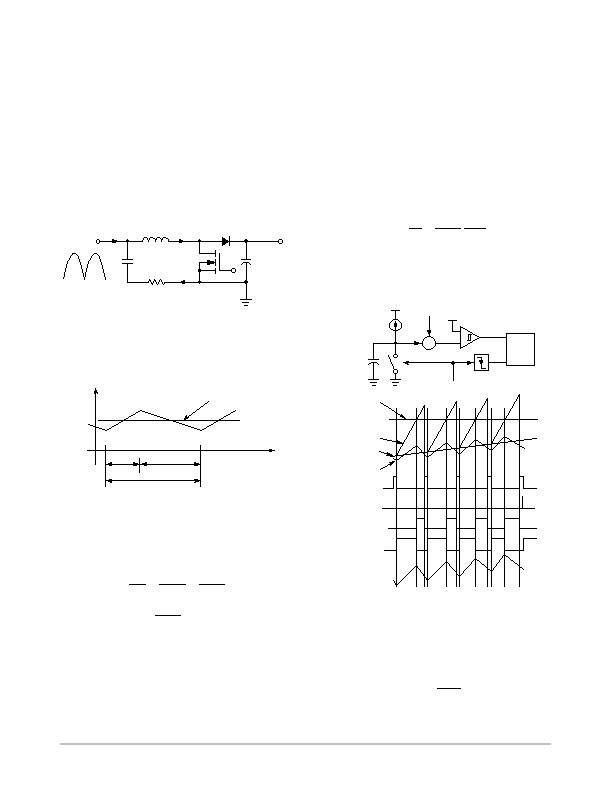
PRINCIPLE OF NCP1654 SCHEME
CCM PFC Boost
A CCM PFC boost converter is shown in Figure 31. The
input voltage is a rectified 50 ro 60 Hz sinusoidal signal.
The MOSFET is switching at a high frequency (typically
65/133/200 kHz in NCP1654) so that the inductor current
I
L
basically consists of high and lowfrequency
components.
Filter capacitor C
filter
is an essential and very small value
capacitor in order to eliminate the highfrequency
component of the inductor I
L
. This filter capacitor cannot
be too bulky because it can pollute the power factor by
distorting the rectified sinusoidal input voltage.
Figure 31. CCM PFC Boost Converter
+
C
bulk
V
in
R
SENSE
C
filter
L
I
in
I
L
V
out
Output
Voltage
PFC Methodology
The NCP1654 uses a proprietary PFC methodology
particularly designed for CCM operation. The PFC
methodology is described in this section.
Figure 32. Inductor Current in CCM
Time
I
in
I
L
t
1
t
2
T
As shown in Figure 32, the inductor current I
L
in a
switching period T includes a charging phase for duration
t
1
and a discharging phase for duration t
2
. The voltage
conversion ratio is obtained in (Equation 1).
V
out
V
in
+
t
1
) t
2
t
2
+
T
T * t
1
(eq. 1)
V
in
+
T * t
1
T
V
out
where
V
out
is the output voltage of PFC stage,
V
in
is the rectified input voltage,
T is the switching period,
t
1
is the MOSFET on time, and
t
2
is the MOSFET off time.
The input filter capacitor C
filter
and the frontended EMI
filter absorbs the highfrequency component of inductor
current I
L
. It makes the input current I
in
a lowfrequency
signal only of the inductor current.
(eq. 2)
I
in
+ I
L*50
where
I
in
is the input AC current.
I
L
is the inductor current.
I
L50
supposes a 50 Hz operation. The suffix 50 means
it is with a 50 Hz bandwidth of the original I
L
.
From (Equation 1) and (Equation 2), the input
impedance Z
in
is formulated.
(eq. 3)
Z
in
+
V
in
I
in
+
T * t
1
T
V
out
I
L*50
where Z
in
is input impedance.
Power factor is corrected when the input impedance Z
in
in (Equation 3) is constant or varies slowly in the 50 or 60
Hz bandwidth.
Figure 33. PFC Duty Modulation and Timing Diagram
+
-
+
I
ch
V
M
V
ref
PFC Modulation
V
ramp
C
ramp
R
S
Q
Clock
0
1
V
ramp
V
ref
V
M
V
M
without
Filtering
Clock
Latch Set
Latch Reset
Output
Inductor
Current
The PFC modulation and timing diagram is shown in
Figure 33. The MOSFET on time t
1
is generated by the
intersection of reference voltage V
REF
and ramp voltage
V
ramp
. A relationship in (Equation 4) is obtained.
(eq. 4)
V
ramp
+ V
m
)
I
ch
t
1
C
ramp
+ V
REF
where
相关PDF资料 |
PDF描述 |
|---|---|
| NCP1927DR2G | IC CTLR PFC/FLYBACK 16-SOIC |
| NCP380HMU21AATBG | IC CURRENT LIMIT SWITCH 6-UDFN |
| NCT1008DMT3R2G | TMP DIO MON/SMBUS 4CH 8WDFN |
| NCT210RQR2G | IC TEMP SENSOR LOC/REM 16QSOP |
| NCT214MT3R2G | IC TEMP SENSOR LOC/REM 10WDFN |
相关代理商/技术参数 |
参数描述 |
|---|---|
| NCP1654BD200R2G | 功能描述:功率因数校正 IC NCP1654 - 200KHZ RoHS:否 制造商:Fairchild Semiconductor 开关频率:300 KHz 最大功率耗散: 最大工作温度:+ 125 C 安装风格:SMD/SMT 封装 / 箱体:SOIC-8 封装:Reel |
| NCP1654BD65R2G | 功能描述:功率因数校正 IC NCP1654-65K-B-SOIC RoHS:否 制造商:Fairchild Semiconductor 开关频率:300 KHz 最大功率耗散: 最大工作温度:+ 125 C 安装风格:SMD/SMT 封装 / 箱体:SOIC-8 封装:Reel |
| NCP1654BP65G | 功能描述:功率因数校正 IC NCP1654-65K-B-PDIP RoHS:否 制造商:Fairchild Semiconductor 开关频率:300 KHz 最大功率耗散: 最大工作温度:+ 125 C 安装风格:SMD/SMT 封装 / 箱体:SOIC-8 封装:Reel |
| NCP1654PFCGEVB | 功能描述:电源管理IC开发工具 NCP1654 PWR FACT CONT EVB RoHS:否 制造商:Maxim Integrated 产品:Evaluation Kits 类型:Battery Management 工具用于评估:MAX17710GB 输入电压: 输出电压:1.8 V |
| NCP1729-SKT | 制造商:P&S 功能描述:Sample Kit, including Two NCP1729SN35T1 and A Development Source CD-ROM 制造商:P&S 功能描述:Sample Kit,including Two NCP1729SN35T1 and A Development Source CD-ROM |
发布紧急采购,3分钟左右您将得到回复。