- 您现在的位置:买卖IC网 > PDF目录22224 > NCP1910B65DWR2G (ON Semiconductor)IC COMBO CTLR ATX 24-SOIC PDF资料下载
参数资料
| 型号: | NCP1910B65DWR2G |
| 厂商: | ON Semiconductor |
| 文件页数: | 25/37页 |
| 文件大小: | 0K |
| 描述: | IC COMBO CTLR ATX 24-SOIC |
| 标准包装: | 1 |
| 模式: | 连续导电(CCM) |
| 频率 - 开关: | 245 kHz |
| 电流 - 启动: | 100µA |
| 安装类型: | 表面贴装 |
| 封装/外壳: | 24-SOIC(0.295",7.50mm 宽)23 引线 |
| 供应商设备封装: | 24-SOIC W |
| 包装: | 标准包装 |
| 其它名称: | NCP1910B65DWR2GOSDKR |
第1页第2页第3页第4页第5页第6页第7页第8页第9页第10页第11页第12页第13页第14页第15页第16页第17页第18页第19页第20页第21页第22页第23页第24页当前第25页第26页第27页第28页第29页第30页第31页第32页第33页第34页第35页第36页第37页
�� �
�
�NCP1910�
�PFC� Reference� Section�
�The� internal� reference� voltage� (V� PREF� )� is� trimmed� to� be�
�±� 2%� accurate� over� the� temperature� range� (the� typical� value�
�is� 2.5� V).� V� PREF� is� the� reference� used� for� the� regulation� of�
�PFC� section.�
�PFC� Feedback� and� Compensation�
�V� CTRL� R� FBL� @� G� EA� R� Z� 1� )� sR� Z� C� Z�
�+� @� (eq.� 17)�
�V� bulk� R� FBL� )� R� FBU� sR� Z� C� Z� 1� )� sR� Z� C� P�
�PFC� Power� Analysis� and� V� in2� Feed� ?� Forward�
�From� Equation� 7� through� 13,� the� input� impedance� Z� in� is�
�re� ?� formulated� in� Equation� 18.�
�V� in�
�V� bulk�
�Z� in� +�
�2R� M� R� SENSE� @� K� LBO� 2� @� V� ac� 2� @� V� bulk� I� L�
�p� 2� R� CS� @� V� CTRL� *� V� CTRL� min� @� V� PREF� I� L� ?� 50�
�(eq.� 18)�
�When� I� L� is� equal� to� I� L� ?� 50� ,� Equation� 18� is� re� ?� formulated� in�
�Equation� 19.�
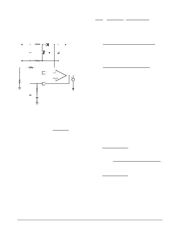
�R� FBL�
�R� FBU�
�FB�
�V� PREF�
�V� CTRL�
�OTA�
�V� CTRL(min)�
�2R� M� R� SENSE� @� K� LBO� 2� @� V� ac� 2� @� V� bulk�
�Z� in� +� (eq.� 19)�
�p� 2� R� CS� @� V� CTRL� *� V� CTRL� min� @� V� PREF�
�The� multiplier� capacitor� C� M� is� the� one� to� filter� the�
�high� ?� frequency� component� of� the� multiplier� voltage� V� M� .�
�The� high� ?� frequency� component� is� basically� coming� from�
�R� Z�
�To� Multiplier� of� V� M� pin�
�C� P�
�C� Z�
�Figure� 49.� V� CTRL� Type� ?� 2� Compensation�
�The� output� voltage� V� bulk� of� the� PFC� circuits� is� sensed� at�
�FB� pin� via� the� resistor� divider� (R� FBL� and� R� FBU� )� as� shown� in�
�Figure� 49.� V� bulk� is� regulated� as� described� in� Equation� 16.�
�the� inductor� current� I� L� .� On� the� other� hand,� the� input� filter�
�capacitor� C� in� similarly� removes� the� high� ?� frequency�
�component� of� inductor� current� I� L� .� If� the� capacitors� C� M� and�
�C� in� match� with� each� other� in� terms� of� filtering� capability,� I� L�
�becomes� I� L� ?� 50� .� Input� impedance� Z� in� is� roughly� constant� over�
�the� bandwidth� of� 50� or� 60� Hz� and� power� factor� is� corrected.�
�Input� and� output� power� (P� in� and� P� out� )� are� derived� in�
�Equations� 20� and� 21� when� the� circuit� efficiency� η� is�
�obtained� or� assumed.� The� variable� V� ac� stands� for� the� rms�
�input� voltage.�
�V� bulk� +� V� PREF�
�p� 2� @� R� CS� @� V� CTRL� *� V� CTRL� min� @� V� PREF�
�V� CTRL� *� V� CTRL� min�
�R� FBU� )� R� FBL�
�(eq.� 16)�
�R� FBL�
�The� feedback� signal� V� FB� represents� the� output� voltage�
�V� bulk� and� will� be� used� in� the� output� voltage� regulation,�
�Over� ?� voltage� protection� (OVP),� fast� transient� response,� and�
�under� ?� voltage� protection� (UVP)�
�The� Operational� Trans� ?� conductance� Amplifier� (OTA)�
�P� in� +�
�T�
�V� ac� 2�
�Z� in� 2R� M� R� SENSE� K� LBO� 2� @� V� bulk�
�+�
�V� bulk�
�(eq.� 20)�
�constructs� a� control� voltage,� V� CTRL� ,� depending� on� the�
�output� power� and� hence� V� bulk� .� The� operating� range� of�
�V� CTRL� is� from� V� CTRL(min)� to� V� CTRL(max)� .� The� signal� used�
�for� PFC� duty� modulation� is� after� decreasing� a� offset� voltage,�
�P� in� +� h� P� in� +� h�
�p� 2� @� R� CS� @� V� CTRL� *� V� CTRL� min� @� V� PREF�
�2R� M� R� SENSE� K� LBO� 2� @� V� bulk�
�V� CTRL� *� V� CTRL� min�
�V� CTRL(min)� ,� i.e.� V� CTRL� ?� V� CTRL(min)� .�
�This� control� voltage� V� CTRL� is� a� roughly� constant� voltage�
�that� comes� from� the� PFC� output� voltage� V� bulk� that� is� a� slowly�
�varying� signal.� The� bandwidth� of� V� CTRL� can� be� additionally�
�limited� by� inserting� the� external� type� ?� 2� compensation�
�components� (that� are� R� Z� ,� C� Z� ,� and� C� P� as� shown� in� Figure� 49).�
�It� is� recommended� to� limit� cross� over� frequency� of� open� loop�
�system� below� 20� Hz� typically� if� the� input� ac� voltage� is� 50� Hz�
�(eq.� 21)�
�T�
�V� bulk�
�Because� of� the� V� in2� feed� ?� forward,� the� power� delivery� is�
�independent� from� input� voltage.� Hence� the� transfer� function�
�of� power� stage� is� independent� from� input� voltage,� which�
�easies� the� compensation� loop� design.�
�to� achieve� power� factor� correction� purpose.�
�The� transformer� of� V� bulk� to� V� CTRL� is� as� described� in�
�Equation� 16� if� C� Z� >>� C� P� .� G� EA� is� the� error� amplifier� gain.�
�http://onsemi.com�
�25�
�相关PDF资料 |
PDF描述 |
|---|---|
| NCP511SN15T1G | IC REG LDO 1.5V .15A 5TSOP |
| AMC19DRTI-S13 | CONN EDGECARD 38POS .100 EXTEND |
| ACC30DRTH-S13 | CONN EDGECARD 60POS DIP .100 SLD |
| VE-J4P-CX-F1 | CONVERTER MOD DC/DC 13.8V 75W |
| NCP1910A65DWR2G | IC COMBO CTLR ATX 24-SOIC |
相关代理商/技术参数 |
参数描述 |
|---|---|
| NCP1910GEVB | 功能描述:电源管理IC开发工具 NCP1910DEMO-B-TLS RoHS:否 制造商:Maxim Integrated 产品:Evaluation Kits 类型:Battery Management 工具用于评估:MAX17710GB 输入电压: 输出电压:1.8 V |
| NCP1927DR2G | 功能描述:功率因数校正 IC PFC AND FLYBACK CONTROLER RoHS:否 制造商:Fairchild Semiconductor 开关频率:300 KHz 最大功率耗散: 最大工作温度:+ 125 C 安装风格:SMD/SMT 封装 / 箱体:SOIC-8 封装:Reel |
| NCP1937A1DR2G | 制造商:ON Semiconductor 功能描述:COMBO PFC & QUAZI FLYBACK - Tape and Reel 制造商:ON Semiconductor 功能描述:REEL / COMBO PFC & QUAZI FLYBACK |
| NCP1937B1DR2G | 制造商:ON Semiconductor 功能描述:COMBO PFC & QUAZI FLYBACK - Tape and Reel |
| NCP1937BADAPGEVB | 制造商:ON Semiconductor 功能描述:ADPTR 90W PFC+QR<10MW - Bulk 制造商:ON Semiconductor 功能描述:BOARD EVAL FOR NCP1937 制造商:ON Semiconductor 功能描述:Power Management IC Development Tools 90 W Adapter PFC+QR 10 MW Eval Brd |
发布紧急采购,3分钟左右您将得到回复。