- 您现在的位置:买卖IC网 > Datasheet目录45 > NCP1927DR2G (ON Semiconductor)IC CTLR PFC/FLYBACK 16-SOIC Datasheet资料下载
参数资料
| 型号: | NCP1927DR2G |
| 厂商: | ON Semiconductor |
| 文件页数: | 22/24页 |
| 文件大小: | 531K |
| 描述: | IC CTLR PFC/FLYBACK 16-SOIC |
| 标准包装: | 2,500 |
| 系列: | * |
NCP1927
http://onsemi.com
22
Go To Standby Pin
The Go To Standby (GTS) pin is used to disable the PFC
stage during system standby based on the flyback stage load
condition. This can be done by connecting it to the flyback
stage feedback pin (FFB) through a resistor divider or by
directly driving the pin with an optocoupler. These
implementations are shown in Figures 29 and 30.
The GTS pin contains an internal pull down resistor, R
GTS
(typically 200 kW), for use with an optocoupler and to
ensure the PFC is disabled if the pin is floating.
Figure 29. GTS Implementation with Feedback Pin
GTS
FFB
R
GTS1
R
GTS2
C
GTS
The resistor divider from the FFB pin is used to setup the
GTS power level threshold. When V
GTS
is brought below
the GTS threshold, V
standby
, the PFC controller stops
switching and enter standby mode. It remains in standby
until V
GTS
is brought above the hysteresis of V
standby
(V
standby(HYS)
). A timer is included on the GTS pin to ensure
transients on the flyback converter do not trigger GTS.
However, the PFC must come out of standby as soon as
possible if there is a request to turn on the TV. Therefore, the
timer is bypassed when coming out of standby. The FFB
voltage at which the PFC enters GTS is expressed using
Equation 21.
V
FFB(GTS)
+ V
GTS
@
R
GTS1
) R
equiv
R
equiv
(eq. 21)
where R
equiv
is the parallel resistor combination of R
GTS
and
R
GTS2
and is calculated using Equation 22.
R
equiv
+
R
GTS
@ R
GTS2
R
GTS
) R
GTS2
(eq. 22)
If direct control of the PFC standby mode is desired, the
GTS pin can instead be driven with an optocoupler from the
secondary side to force the PFC stage in and out of standby
mode. A resistor (R
limit
) is placed in series with the
optocoupler to limit the current into the GTS pin.
Figure 30. GTS Implementation with Optocoupler
VCC_AUX
GTS
C
GTS
from secondary side
R
limit
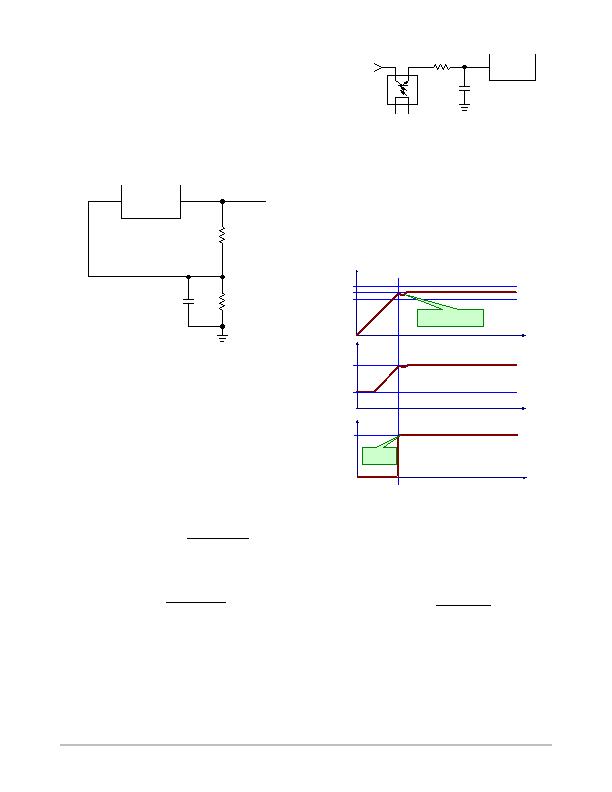
IENABLE Pin
The IENABLE pin is designed to drive an optocoupler
that enables the Flat Panel TV backlight inverter once the
PFC stage reaches regulation. The NCP1927 achieves this
by monitoring the current sourced by the EA. Once this
current drops to 0 mA, the IENABLE pin voltage switches
to V
IENABLE(high)
(typically 5.0 V). This operation is shown
in Figure 31.
Figure 31. IENABLE Pin Timing
time
V
out
V
out(MAX)
time
V
IENABLE
5 V
0 V
V
out(MIN)
V
out(NOM)
time
I
EA(out)
0 糀
20 糀
Inverter
Starts
Undershoot from Inverter
Load
A separate comparator on the PFB pin is used to protect
the inverter from undervoltage conditions by detecting
when the PFB voltage falls below V
disable
. When this occurs,
the IENABLE pin voltage switches to V
IENABLE(low)
. Using
the result from Equation 7, the output threshold that sets the
IENABLE pin low can be calculated with Equation 23.
V
out(disable)
+
V
out
@ V
disable
V
REF
(eq. 23)
where V
disable
is the disable threshold (1.865 V typical).
The IENABLE pin can also be used as a voltage reference.
To filter noise, a decoupling capacitor (C
REF
) may be
connected to the pin.
相关PDF资料 |
PDF描述 |
|---|---|
| NCP380HMU21AATBG | IC CURRENT LIMIT SWITCH 6-UDFN |
| NCT1008DMT3R2G | TMP DIO MON/SMBUS 4CH 8WDFN |
| NCT210RQR2G | IC TEMP SENSOR LOC/REM 16QSOP |
| NCT214MT3R2G | IC TEMP SENSOR LOC/REM 10WDFN |
| NCT72CMNR2G | IC REMOTE THERMAL SENSOR 8-DFN |
相关代理商/技术参数 |
参数描述 |
|---|---|
| NCP1937A1DR2G | 制造商:ON Semiconductor 功能描述:COMBO PFC & QUAZI FLYBACK - Tape and Reel 制造商:ON Semiconductor 功能描述:REEL / COMBO PFC & QUAZI FLYBACK |
| NCP1937B1DR2G | 制造商:ON Semiconductor 功能描述:COMBO PFC & QUAZI FLYBACK - Tape and Reel |
| NCP1937BADAPGEVB | 制造商:ON Semiconductor 功能描述:ADPTR 90W PFC+QR<10MW - Bulk 制造商:ON Semiconductor 功能描述:BOARD EVAL FOR NCP1937 制造商:ON Semiconductor 功能描述:Power Management IC Development Tools 90 W Adapter PFC+QR 10 MW Eval Brd |
| NCP21WB333 | 制造商:MURATA 制造商全称:Murata Manufacturing Co., Ltd. 功能描述:for Surface Mounting Application |
| NCP21WB333J03RA | 功能描述:热敏电阻 - NTC 33K OHM 5% RoHS:否 制造商:EPCOS 电阻:10 kOhms 功率额定值:150 mW 容差:2 % 端接类型:Radial 系列:B57703M 工作温度范围:- 55 C to + 125 C |
发布紧急采购,3分钟左右您将得到回复。