- 您现在的位置:买卖IC网 > PDF目录15259 > NCP302LSN09T1G (ON Semiconductor)IC VOLT DETECT CMOS 0.9V 5TSOP PDF资料下载
参数资料
| 型号: | NCP302LSN09T1G |
| 厂商: | ON Semiconductor |
| 文件页数: | 1/26页 |
| 文件大小: | 0K |
| 描述: | IC VOLT DETECT CMOS 0.9V 5TSOP |
| 标准包装: | 1 |
| 类型: | 简单复位/加电复位 |
| 监视电压数目: | 1 |
| 输出: | 推挽式,图腾柱 |
| 复位: | 低有效 |
| 复位超时: | 可调节/可选择 |
| 电压 - 阀值: | 0.9V |
| 工作温度: | -40°C ~ 85°C |
| 安装类型: | 表面贴装 |
| 封装/外壳: | 6-TSOP(0.059",1.50mm 宽)5 引线 |
| 供应商设备封装: | 5-TSOP |
| 包装: | 剪切带 (CT) |
| 其它名称: | NCP302LSN09T1GOSCT |
�� �
�
�NCP302,� NCP303�
�Voltage� Detector� Series�
�with� Programmable� Delay�
�The� NCP302� and� NCP303� series� are� second� generation� ultra� ?� low�
�current� voltage� detectors� that� contain� a� programmable� time� delay�
�generator.� These� devices� are� specifically� designed� for� use� as� reset�
�controllers� in� portable� microprocessor� based� systems� where� extended�
�battery� life� is� paramount.�
�Each� series� features� a� highly� accurate� undervoltage� detector� with�
�hysteresis� and� an� externally� programmable� time� delay� generator.� This�
�http://onsemi.com�
�MARKING�
�DIAGRAM�
�combination� of� features� prevents� erratic� system� reset� operation.�
�The� NCP302� series� consists� of� complementary� output� devices� that�
�are� available� with� either� an� active� high� or� active� low� reset.� The�
�NCP303� series� has� an� open� drain� N� ?� Channel� output� with� an� active� low�
�reset� output.�
�5�
�1�
�TSOP� ?� 5/�
�SOT23� ?� 5�
�CASE� 483�
�5�
�1�
�xxx� AYW� G�
�G�
�1�
�5� C� D�
�Features�
�?� Quiescent� Current� of� 0.5� m� A� Typical�
�?� High� Accuracy� Undervoltage� Threshold� of� 2.0%�
�?� Externally� Programmable� Time� Delay� Generator�
�?� Wide� Operating� Voltage� Range� of� 0.8� V� to� 10� V�
�?� Complementary� or� Open� Drain� Output�
�?� Active� Low� or� Active� High� Reset�
�?� Specified� Over� the� ?� 40� °� C� to� +125� °� C� Temperature� Range�
�(Except� for� Voltage� Options� from� 0.9� to� 1.1� V)�
�?� NCV� Prefix� for� Automotive� and� Other� Applications� Requiring�
�Unique� Site� and� Control� Change� Requirements;� AEC� ?� Q100�
�Qualified� and� PPAP� Capable�
�?� These� Devices� are� Pb� ?� Free� and� are� RoHS� Compliant�
�Typical� Applications�
�?� Microprocessor� Reset� Controller�
�?� Low� Battery� Detection�
�?� Power� Fail� Indicator�
�?� Battery� Backup� Detection�
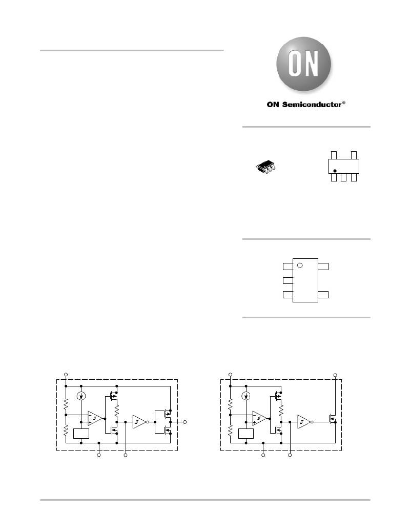
�NCP302xSNxxT1�
�Complementary� Output� Configuration�
�xxx� =� Specific� Device� Code�
�A� =� Assembly� Location�
�Y� =� Year�
�W� =� Work� Week�
�G� =� Pb� ?� Free� Package�
�(Note:� Microdot� may� be� in� either� location)�
�PIN� CONNECTIONS�
�Reset�
�Output�
�Input� 2�
�Ground� 3� 4� N.C.�
�(Top� View)�
�ORDERING� INFORMATION�
�See� detailed� ordering� and� shipping� information� in� the� ordering�
�information� section� on� page� 22� of� this� data� sheet.�
�NCP303LSNxxT1�
�Open� Drain� Output� Configuration�
�2�
�Input�
�2�
�Input�
�1�
�Reset� Output�
�R� D�
�1�
�R� D�
�V� ref�
�*�
�Reset�
�Output�
�V� ref�
�3�
�GND� 5�
�C� D�
�3�
�GND� 5�
�C� D�
�*� Inverter� for� active� low� devices.�
�*� Buffer� for� active� high� devices.�
�This� device� contains� 28� active� transistors.�
�Figure� 1.� Representative� Block� Diagrams�
�?� Semiconductor� Components� Industries,� LLC,� 2013�
�May,� 2013� ?� Rev.� 25�
�1�
�Publication� Order� Number:�
�NCP302/D�
�相关PDF资料 |
PDF描述 |
|---|---|
| RCM22DRMD-S288 | CONN EDGECARD 44POS .156 EXTEND |
| RBA18DRMT-S288 | CONN EDGECARD 36POS .125 EXTEND |
| ESM12DTKT-S288 | CONN EDGECARD 24POS .156 EXTEND |
| ECM28DRSN-S288 | CONN EDGECARD 56POS .156 EXTEND |
| ECM28DRSH-S288 | CONN EDGECARD 56POS .156 EXTEND |
相关代理商/技术参数 |
参数描述 |
|---|---|
| NCP302LSN10T1 | 制造商:Rochester Electronics LLC 功能描述:- Bulk 制造商:ON Semiconductor 功能描述: |
| NCP302LSN11T1 | 制造商:Rochester Electronics LLC 功能描述:- Bulk 制造商:ON Semiconductor 功能描述: |
| NCP302LSN12T1 | 制造商:Rochester Electronics LLC 功能描述:- Bulk 制造商:Motorola Inc 功能描述: 制造商:ON Semiconductor 功能描述: 制造商:MOTOROLA 功能描述: |
| NCP302LSN13T1 | 制造商:Rochester Electronics LLC 功能描述:- Bulk |
| NCP302LSN14T1 | 制造商:Rochester Electronics LLC 功能描述:- Tape and Reel 制造商:ON Semiconductor 功能描述: |
发布紧急采购,3分钟左右您将得到回复。