- 您现在的位置:买卖IC网 > PDF目录15259 > NCP302LSN09T1G (ON Semiconductor)IC VOLT DETECT CMOS 0.9V 5TSOP PDF资料下载
参数资料
| 型号: | NCP302LSN09T1G |
| 厂商: | ON Semiconductor |
| 文件页数: | 16/26页 |
| 文件大小: | 0K |
| 描述: | IC VOLT DETECT CMOS 0.9V 5TSOP |
| 标准包装: | 1 |
| 类型: | 简单复位/加电复位 |
| 监视电压数目: | 1 |
| 输出: | 推挽式,图腾柱 |
| 复位: | 低有效 |
| 复位超时: | 可调节/可选择 |
| 电压 - 阀值: | 0.9V |
| 工作温度: | -40°C ~ 85°C |
| 安装类型: | 表面贴装 |
| 封装/外壳: | 6-TSOP(0.059",1.50mm 宽)5 引线 |
| 供应商设备封装: | 5-TSOP |
| 包装: | 剪切带 (CT) |
| 其它名称: | NCP302LSN09T1GOSCT |
�� �
�
�NCP302,� NCP303�
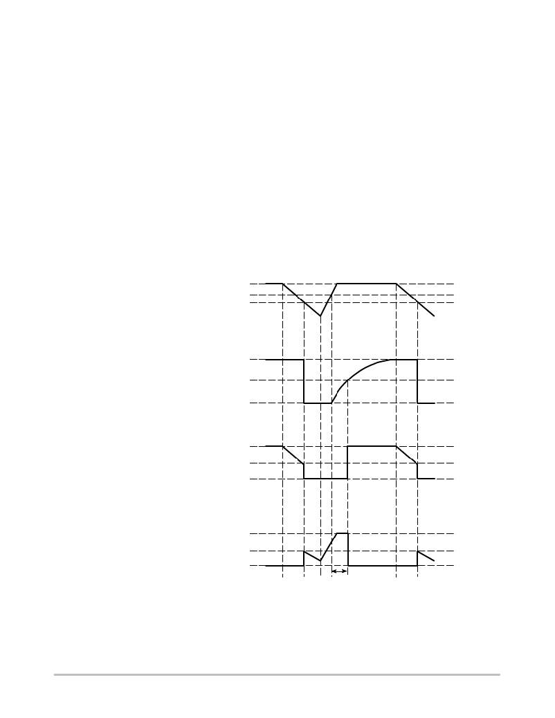
�OPERATING� DESCRIPTION�
�The� NCP302� and� NCP303� series� devices� consist� of� a�
�precision� voltage� detector� that� drives� a� time� delay� generator.�
�Figures� 37� and� 38� show� a� timing� diagram� and� a� typical�
�application.� Initially� consider� that� input� voltage� V� in� is� at� a�
�nominal� level� and� it� is� greater� than� the� voltage� detector� upper�
�threshold� (V� DET+� ).� The� voltage� at� Pin� 5� and� capacitor� C� D�
�will� be� at� the� same� level� as� V� in� ,� and� the� reset� output� (Pin� 1)�
�will� be� in� the� high� state� for� active� low� devices,� or� in� the� low�
�state� for� active� high� devices.� If� there� is� a� power� interruption�
�and� V� in� becomes� significantly� deficient,� it� will� fall� below� the�
�lower� detector� threshold� (V� DET� ?� )� and� the� external� time�
�delay� capacitor� C� D� will� be� immediately� discharged� by� an�
�internal� N� ?� Channel� MOSFET� that� connects� to� Pin� 5.� This�
�sequence� of� events� causes� the� Reset� output� to� be� in� the� low�
�state� for� active� low� devices,� or� in� the� high� state� for� active�
�high� devices.� After� completion� of� the� power� interruption,�
�V� in� will� again� return� to� its� nominal� level� and� become� greater�
�than� the� V� DET+� .� The� voltage� detector� will� turn� off� the�
�N� ?� Channel� MOSFET� and� allow� pullup� resistor� R� D� to� charge�
�external� capacitor� C� D� ,� thus� creating� a� programmable� delay�
�for� releasing� the� reset� signal.� When� the� voltage� at� Pin� 5�
�exceeds� the� inverter/buffer� threshold,� typically� 0.675� V� in� ,�
�the� reset� output� will� revert� back� to� its� original� state.� The� reset�
�output� time� delay� versus� capacitance� is� shown� in� Figures� 30�
�through� 32.� The� voltage� detector� and� inverter/buffer� have�
�built� ?� in� hysteresis� to� prevent� erratic� reset� operation.�
�Although� these� device� series� are� specifically� designed� for�
�use� as� reset� controllers� in� portable� microprocessor� based�
�systems,� they� offer� a� cost� ?� effective� solution� in� numerous�
�applications� where� precise� voltage� monitoring� and� time�
�delay� are� required.� Figures� 38� through� 46� show� various�
�application� examples.�
�Input� Voltage,� Pin� 2�
�Capacitor,� Pin� 5�
�Reset� Output� (Active� Low),� Pin� 1�
�Reset� Output� (Active� High),� Pin� 1�
�V� in�
�V� DET� +�
�V� DET� ?�
�V� in�
�0.675� V� in�
�V� in�
�V� DET� ?�
�0V�
�V� in�
�V� DET� ?�
�0V�
�Figure� 37.� Timing� Waveforms�
�http://onsemi.com�
�16�
�t� D2�
�相关PDF资料 |
PDF描述 |
|---|---|
| RCM22DRMD-S288 | CONN EDGECARD 44POS .156 EXTEND |
| RBA18DRMT-S288 | CONN EDGECARD 36POS .125 EXTEND |
| ESM12DTKT-S288 | CONN EDGECARD 24POS .156 EXTEND |
| ECM28DRSN-S288 | CONN EDGECARD 56POS .156 EXTEND |
| ECM28DRSH-S288 | CONN EDGECARD 56POS .156 EXTEND |
相关代理商/技术参数 |
参数描述 |
|---|---|
| NCP302LSN10T1 | 制造商:Rochester Electronics LLC 功能描述:- Bulk 制造商:ON Semiconductor 功能描述: |
| NCP302LSN11T1 | 制造商:Rochester Electronics LLC 功能描述:- Bulk 制造商:ON Semiconductor 功能描述: |
| NCP302LSN12T1 | 制造商:Rochester Electronics LLC 功能描述:- Bulk 制造商:Motorola Inc 功能描述: 制造商:ON Semiconductor 功能描述: 制造商:MOTOROLA 功能描述: |
| NCP302LSN13T1 | 制造商:Rochester Electronics LLC 功能描述:- Bulk |
| NCP302LSN14T1 | 制造商:Rochester Electronics LLC 功能描述:- Tape and Reel 制造商:ON Semiconductor 功能描述: |
发布紧急采购,3分钟左右您将得到回复。