参数资料
| 型号: | NCP5217AMNTXG |
| 厂商: | ON Semiconductor |
| 文件页数: | 10/16页 |
| 文件大小: | 0K |
| 描述: | IC REG CTRLR BUCK PWM 14-QFN |
| 标准包装: | 3,000 |
| PWM 型: | 电流/电压模式 |
| 输出数: | 1 |
| 频率 - 最大: | 330kHz |
| 电源电压: | 4.5 V ~ 27 V |
| 降压: | 是 |
| 升压: | 无 |
| 回扫: | 无 |
| 反相: | 无 |
| 倍增器: | 无 |
| 除法器: | 无 |
| Cuk: | 无 |
| 隔离: | 无 |
| 工作温度: | -40°C ~ 85°C |
| 封装/外壳: | 14-VFQFN 裸露焊盘 |
| 包装: | 带卷 (TR) |
| 其它名称: | NCP5217AMNTXG-ND NCP5217AMNTXGOSTR |
�� �
�
�NCP5217A�
�The� Figure� 18� shows� how� to� realize� the� AVP� function.� A�
�current� path� is� connecting� to� the� FB� pin� via� R� ocp� resistor.�
�Rocp� is� not� actually� for� AVP� function,� indeed,� R� ocp� is� used�
�for� OCP� threshold� value� programming.� The� IDRP/OCP� pin�
�has� dual� functions:� OCP� programming� and� AVP.� At� the�
�IDRP/OCP� pin,� conceptually� there� is� a� current� source� which�
�is� modulated� by� current� sensing� amplifier.�
�The� output� voltage� Vo� with� AVP� is:�
�V� O� +� V� O� 0� *� I� O� *� R� LL�
�(eq.� 1)�
�Where� I� o� is� the� load� current,� no� load� output� voltage� Vo0� is�
�set� by� the� external� divider� that� is�
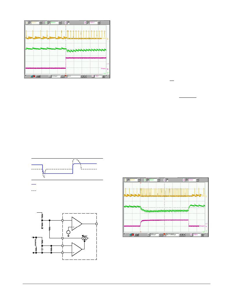
�Top� to� Bottom� SWN,� V� o� ,� Transient� Signal�
�V� O� 0� +� 1� )�
�Rt�
�Rb�
�*� V� ref�
�(eq.� 2)�
�Figure� 16.� Transient� Response� with� TRE� Enable�
�The� load� line� impendence� R� LL� is� given� by:�
�Adaptive� Voltage� Positioning� (AVP)�
�R� LL� +� DCR� *� Gain_CS� *� Rt� *�
�Rs2�
�Rs1� )� Rs2�
�(eq.� 3)�
�For� applications� with� fast� transient� currents,� adaptive�
�voltage� positioning� can� reduce� peak� ?� to� ?� peak� output� voltage�
�deviations� due� to� load� transients.� With� the� use� of� AVP,� the�
�output� voltage� allows� to� have� some� controlled� sag� when� load�
�current� is� applied.� Upon� removal� of� the� load,� the� output�
�voltage� returns� no� higher� than� the� original� level,� just�
�allowing� one� output� transient� peak� to� be� cancelled� over� a�
�load� step� up� and� release� cycle.� The� amount� of� AVP� is�
�adjustable.�
�The� behaviors� of� the� V� o� waveforms� with� or� without� AVP�
�are� depicted� at� Figure� 17.�
�Where� DCR� is� inductor� DC� resistance.� Gain_CS� is� a� gain�
�from� [(CS+)� ?� (CS� ?� )]� to� IDRP� Gain� (At� electrical� table,� the�
�symbol� is� IDRP_GAIN),� the� typical� value� is� 0.525� m� A/mV.�
�The� AVP� function� can� be� easily� disable� by� shorting� the�
�Rocp� resistor� into� ground.�
�From� the� equation� we� can� see� that� the� value� of� “top”�
�resistor� Rt� can� affect� the� R� LL� ,� so� it� is� recommended� to� define�
�the� amount� of� R� LL� FRIST� before� defining� the� compensation�
�component� value.� And� if� the� user� wants� to� fine� tune� the�
�compensation� network� for� optimizing� the� transient�
�performance,� it� is� NOT� recommend� to� adjust� the� value� of� Rt.�
�Otherwise,� both� transient� performance� and� AVP� amount�
�will� be� affected.� The� following� diagram� shows� the� typical�
�waveform� of� AVP.� Note� that� the� Rt� typical� value� should� be�
�above� 1� k� W� .�
�Vo� With� AVP�
�Vo� Without� AVP�
�Figure� 17.� Adaptive� Voltage� Positioning�
�Vo�
�Rt�
�Rb�
�FB�
�+�
�COMP�
�?� Vref�
�Rocp�
�IDRP/OCP�
�+�
�IDRP�
�DCR�
�L�
�Rs1�
�Cs�
�CS+�
�Rs2�
�CS� ?�
�+�
�Gi�
�Top� to� Bottom:� SWN,� V� o� ,� Transient� Signal� (0.5� ?� 10� ?� 0.5A)�
�Figure� 19.� Typical� waveform� of� AVP�
�Figure� 18.� Configuration� for� AVP� function�
�http://onsemi.com�
�10�
�相关PDF资料 |
PDF描述 |
|---|---|
| NCP5218MNR2G | IC DDR PWR CTLR 2IN2 NTBK 22-DFN |
| NCP5220MNR2G | IC CTLR PWM DUAL BUCK PWR 20-DFN |
| NCP5222MNR2G | IC CTLR BUCK 2CH 2PH 28QFN |
| NCP5252MNTXG | IC REG BUCK SYNC ADJ 2A 16QFN |
| NCP5314FTR2G | IC CTLR CPU 2/3/4 PHASE 32-LQFP |
相关代理商/技术参数 |
参数描述 |
|---|---|
| NCP5218 | 制造商:ONSEMI 制造商全称:ON Semiconductor 功能描述:2−in−1 Notebook DDR Power Controller |
| NCP5218MNR2G | 功能描述:电压模式 PWM 控制器 2IN1 NOTEBK DDR CNTL RoHS:否 制造商:Texas Instruments 输出端数量:1 拓扑结构:Buck 输出电压:34 V 输出电流: 开关频率: 工作电源电压:4.5 V to 5.5 V 电源电流:600 uA 最大工作温度:+ 125 C 最小工作温度:- 40 C 封装 / 箱体:WSON-8 封装:Reel |
| NCP5220 | 制造商:ONSEMI 制造商全称:ON Semiconductor 功能描述:3−in−1 PWM Dual Buck and Linear Power Controller |
| NCP5220AMNR2 | 功能描述:DC/DC 开关控制器 3-in-1 PWM Dual Buck RoHS:否 制造商:Texas Instruments 输入电压:6 V to 100 V 开关频率: 输出电压:1.215 V to 80 V 输出电流:3.5 A 输出端数量:1 最大工作温度:+ 125 C 安装风格: 封装 / 箱体:CPAK |
| NCP5220AMNR2G | 功能描述:DC/DC 开关控制器 ANA DDR PWER CNTRLR RoHS:否 制造商:Texas Instruments 输入电压:6 V to 100 V 开关频率: 输出电压:1.215 V to 80 V 输出电流:3.5 A 输出端数量:1 最大工作温度:+ 125 C 安装风格: 封装 / 箱体:CPAK |
发布紧急采购,3分钟左右您将得到回复。