- 您现在的位置:买卖IC网 > PDF目录20398 > NCP5355DR2G (ON Semiconductor)IC DRVR MOSF SYNC BUCK 12V 8SOIC PDF资料下载
参数资料
| 型号: | NCP5355DR2G |
| 厂商: | ON Semiconductor |
| 文件页数: | 3/10页 |
| 文件大小: | 0K |
| 描述: | IC DRVR MOSF SYNC BUCK 12V 8SOIC |
| 产品变化通告: | Product Discontinuation 01/Oct/2008 |
| 标准包装: | 2,500 |
| 配置: | 高端和低端,同步 |
| 输入类型: | 反相和非反相 |
| 延迟时间: | 30ns |
| 电流 - 峰: | 2A |
| 配置数: | 1 |
| 输出数: | 2 |
| 高端电压 - 最大(自引导启动): | 26V |
| 电源电压: | 9.2 V ~ 13.2 V |
| 工作温度: | 0°C ~ 125°C |
| 安装类型: | 表面贴装 |
| 封装/外壳: | 8-SOIC(0.154",3.90mm 宽) |
| 供应商设备封装: | 8-SOICN |
| 包装: | 带卷 (TR) |
| 其它名称: | NCP5355DR2GOS |
�� �
�
�NCP5355�
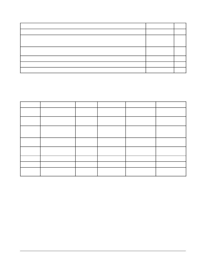
�MAXIMUM� RATINGS�
�Rating�
�Operating� Junction� Temperature,� T� J�
�Package� Thermal� Resistance:� SOIC?8�
�Junction?to?Case,� R� q� JC�
�Junction?to?Ambient,� R� q� JA�
�Package� Thermal� Resistance:� SOIC?8� EP�
�Junction?to?Ambient,� R� q� JA� (Note� 1)�
�Storage� Temperature� Range,� T� S�
�Lead� Temperature� Soldering:� Reflow:� (SMD� styles� only)� (Note� 2)�
�JEDEC� Moisture� Sensitivity�
�Value�
�Internally� Limited�
�45�
�165�
�50�
�?65� to� 150�
�230� peak�
�1�
�Unit�
�°� C�
�°� C/W�
�°� C/W�
�°� C/W�
�°� C�
�°� C�
�?�
�Maximum� ratings� are� those� values� beyond� which� device� damage� can� occur.� Maximum� ratings� applied� to� the� device� are� individual� stress� limit�
�values� (not� normal� operating� conditions)� and� are� not� valid� simultaneously.� If� these� limits� are� exceeded,� device� functional� operation� is� not� implied,�
�damage� may� occur� and� reliability� may� be� affected.�
�NOTE:� This� device� is� ESD� sensitive.� Use� standard� ESD� precautions� when� handling.�
�1.� Ratings� applies� when� soldered� to� an� appropriate� thermal� area� on� the� PCB.�
�2.� 60� seconds� maximum� above� 183� °� C.�
�MAXIMUM� RATINGS�
�Pin� Symbol�
�V� S�
�Pin� Name�
�Main� Supply� Voltage� Input�
�V� MAX�
�15� V�
�V� MIN�
�?0.3� V�
�I� SOURCE�
�NA�
�I� SINK�
�2.0� A� Peak� (<� 100� m� s)�
�250� mA� DC�
�BST�
�Bootstrap� Supply� Voltage�
�30� V� wrt/PGND�
�?0.3� V� wrt/DRN�
�NA�
�2.0� A� Peak� (<� 100� m� s)�
�Input�
�15� V� wrt/DRN�
�250� mA� DC�
�DRN�
�Switching� Node�
�26� V�
�?1.0� V� DC�
�2.0� A� Peak� (<� 100� m� s)�
�NA�
�(Bootstrap� Supply� Return)�
�?5.0� V� for� 100� ns�
�?6.0� V� for� 20� ns�
�250� mA� DC�
�TG�
�BG�
�High?Side� Driver� Output�
�(Top� Gate)�
�Low?Side� Driver� Output�
�30� V� wrt/PGND�
�15� V� wrt/DRN�
�15� V�
�?0.3� V� wrt/DRN�
�?0.3� V�
�2.0� A� Peak� (<� 100� m� s)�
�250� mA� DC�
�2.0� A� Peak� (<� 100� m� s)�
�2.0� A� Peak� (<� 100� m� s)�
�250� mA� DC�
�2.0� A� Peak� (<� 100� m� s)�
�(Bottom� Gate)�
�250� mA� DC�
�250� mA� DC�
�CO�
�EN�
�PGND�
�TG� and� BG� Control� Input�
�Enable� Input�
�Ground�
�5.5� V�
�5.5� V�
�0V�
�?0.3� V�
�?0.3� V�
�0V�
�1.0� mA�
�1.0� mA�
�2.0� A� Peak� (<� 100� m� s)�
�1.0� mA�
�1.0� mA�
�NA�
�250� mA� DC�
�NOTE:�
�All� voltages� are� with� respect� to� PGND� except� where� noted.�
�http://onsemi.com�
�3�
�相关PDF资料 |
PDF描述 |
|---|---|
| HBC05DRTI-S13 | CONN EDGECARD 10POS .100 EXTEND |
| V10P10HE3/86A | DIODE SCHOTTKY 10A 100V SMPC |
| R0.25S-3.33.3/HP-R | CONV DC/DC 0.25W 3.3VIN 3.3VOUT |
| LQH2MCN4R7M02L | INDUCTOR 4.7UH 300MA 0806 |
| T95D157M016HZAS | CAP TANT 150UF 16V 20% 2917 |
相关代理商/技术参数 |
参数描述 |
|---|---|
| NCP5355PDR2 | 功能描述:功率驱动器IC 12V 2A Buck Power RoHS:否 制造商:Micrel 产品:MOSFET Gate Drivers 类型:Low Cost High or Low Side MOSFET Driver 上升时间: 下降时间: 电源电压-最大:30 V 电源电压-最小:2.75 V 电源电流: 最大功率耗散: 最大工作温度:+ 85 C 安装风格:SMD/SMT 封装 / 箱体:SOIC-8 封装:Tube |
| NCP5358MNTXG | 功能描述:开关变换器、稳压器与控制器 GATE DRIVERS FOR NOTEBOOK RoHS:否 制造商:Texas Instruments 输出电压:1.2 V to 10 V 输出电流:300 mA 输出功率: 输入电压:3 V to 17 V 开关频率:1 MHz 工作温度范围: 安装风格:SMD/SMT 封装 / 箱体:WSON-8 封装:Reel |
| NCP5359 | 制造商:ONSEMI 制造商全称:ON Semiconductor 功能描述:Gate Driver for Notebook Power Systems |
| NCP5359A | 制造商:ONSEMI 制造商全称:ON Semiconductor 功能描述:Gate Driver for Notebook Power Systems |
| NCP5359ADR2G | 功能描述:功率驱动器IC DUAL MOSFET GATE DRIVER RoHS:否 制造商:Micrel 产品:MOSFET Gate Drivers 类型:Low Cost High or Low Side MOSFET Driver 上升时间: 下降时间: 电源电压-最大:30 V 电源电压-最小:2.75 V 电源电流: 最大功率耗散: 最大工作温度:+ 85 C 安装风格:SMD/SMT 封装 / 箱体:SOIC-8 封装:Tube |
发布紧急采购,3分钟左右您将得到回复。