参数资料
| 型号: | NCS36000DG |
| 厂商: | ON Semiconductor |
| 文件页数: | 5/8页 |
| 文件大小: | 0K |
| 描述: | IC PIR DETECTOR CTLR 14SOIC |
| 标准包装: | 55 |
| 类型: | 检测器控制器 |
| 输入类型: | 数字 |
| 输出类型: | 数字 |
| 接口: | CMOS |
| 电流 - 电源: | 50µA |
| 安装类型: | 表面贴装 |
| 封装/外壳: | 14-SOIC(0.154",3.90mm 宽) |
| 供应商设备封装: | 14-SOICN |
| 包装: | 托盘 |
NCS36000
http://onsemi.com
5
4
+
5
3
+
2
1
G
D
VREF
LDO
6
Sensor dependent
components
Vm
VREF 6
Vm
Vh
Vl
Application dependent
components
+
Vl
Vh
OP2_O
+
Comp_P
Comp_N
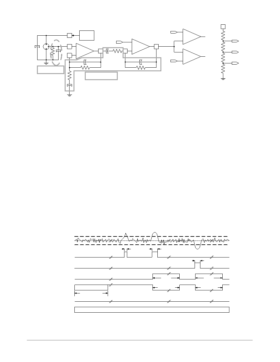
Figure 5. Figure Showing Simplified Block Diagram of Analog Conditioning Stages
Digital Signal Processing Block (all times assume a
62.5 Hz system oscillator frequency)
The digital signaling processing block performs three
major functions.
The first function is that the device toggles LED during the
startup sequencing at approximately two hertz regardless
of the state of the XLED_EN pin. The startup sequence lasts
for thirty seconds. During that time the OUT pin is held low
regardless of the state of OP2_O.
The second function of the digital signal processing block
is to insure a certain glitch width is seen before OUT is
toggled. The digital signal processing block is synchronous
with the system oscillator frequency and therefore the
deglitch time is related to when the comparators toggle
within the oscillator period. A signal width less than two
clock period is guaranteed to be deglitched as a zero. A
signal width of greater than three clock cycles is guaranteed
to be deglitched. It should be noted that downsampling
can occur if sufficient antialiasing is not performed at the
input of the circuit (OPI_P) or if noise is injected into the
amplifiers, an example would be a noisy power supply.
The third function of the digital signal processing block is
to recognize different pulse signatures coming from the
window comparator block. The device is equipped with two
pulse recognition routines. Single pulse mode (MODE tied
to VSS) will trigger the OUT pin if either comparator toggles
and the deglitch time is of the appropriate length. (See
two pulses with each pulse coming from the opposite
comparator to occur within a timeout window of five
seconds (See Figure 7). If the adjacent pulses occur outside
the timeout window then the digital processing block will
restart the pulse recognition routine (Figure 8).
xLED_EN Pin
The xLED_EN pin enables the LED output driver when
motion has been detected. If xLED_EN is tied high the LED
pin will not toggle after motion is detected. If the xLED_EN
is tied low the LED pin will toggle when motion is detected.
During start-up the LED pin will toggle irrespective of how
the xLED_EN pin is tied. (See Figure 6).
OSC
LED
Startup Sequencing
COMP_P
OUT
COMP_N
<32m Sec
>48m Sec
~1.6 Sec
If xLED_EN = 0
MODE
OP2_O
Figure 6. Timing Diagram for SinglePulse Mode Detection
相关PDF资料 |
PDF描述 |
|---|---|
| NCS6415DWR2G | IC VIDEO SWITCH 8X6 20SOIC |
| NCS6416DWR2G | IC VIDEO SWITCH 8X6 20SOIC |
| NCS6433DTBR2G | IC VIDEO SW QUAD 2:1 16-TSSOP |
| NCV1124DG | IC SENSOR DUAL VAR-RELUCT 8-SOIC |
| NCV7001DWG | IC SENSOR VAR RELUCT QUAD 24SOIC |
相关代理商/技术参数 |
参数描述 |
|---|---|
| NCS36000DRG | 功能描述:LED照明驱动器 PIR ASSP RoHS:否 制造商:STMicroelectronics 输入电压:11.5 V to 23 V 工作频率: 最大电源电流:1.7 mA 输出电流: 最大工作温度: 安装风格:SMD/SMT 封装 / 箱体:SO-16N |
| NCS37000 | 制造商:ONSEMI 制造商全称:ON Semiconductor 功能描述:Ground Fault Circuit Interrupter (GFCI) |
| NCS37000DBG | 制造商:ON Semiconductor 功能描述:GFCI NON ST TSSOP - Rail/Tube |
| NCS37000DBRG | 制造商:ON Semiconductor 功能描述:GFCI NON ST TSSOP - Tape and Reel |
| NCS37000MNG | 功能描述:电流和电力监控器、调节器 GFCI ST ASSP RoHS:否 制造商:STMicroelectronics 产品:Current Regulators 电源电压-最大:48 V 电源电压-最小:5.5 V 工作温度范围:- 40 C to + 150 C 安装风格:SMD/SMT 封装 / 箱体:HPSO-8 封装:Reel |
发布紧急采购,3分钟左右您将得到回复。