- 您现在的位置:买卖IC网 > PDF目录20813 > NCV3066DR2G (ON Semiconductor)IC LED DRIVER HIGH BRIGHT 8-SOIC PDF资料下载
参数资料
| 型号: | NCV3066DR2G |
| 厂商: | ON Semiconductor |
| 文件页数: | 7/20页 |
| 文件大小: | 0K |
| 描述: | IC LED DRIVER HIGH BRIGHT 8-SOIC |
| 标准包装: | 2,500 |
| 恒定电流: | 是 |
| 拓扑: | PWM,降压(降压),升压(升压) |
| 输出数: | 1 |
| 内部驱动器: | 是 |
| 类型 - 主要: | 车载 |
| 类型 - 次要: | 高亮度 LED(HBLED) |
| 频率: | 100kHz ~ 250kHz |
| 电源电压: | 3 V ~ 40 V |
| 安装类型: | 表面贴装 |
| 封装/外壳: | 8-SOIC(0.154",3.90mm 宽) |
| 供应商设备封装: | 8-SOICN |
| 包装: | 带卷 (TR) |
| 工作温度: | -40°C ~ 125°C |
�� �
�
�NCP3066,� NCV3066�
�INTRODUCTION�
�The� NCP3066� is� a� monolithic� power� switching� regulator�
�optimized� for� LED� Driver� applications.� Its� flexible�
�architecture� enables� the� system� designer� to� directly�
�implement� step� ?� up,� step� ?� down,� and� voltage� ?� inverting�
�converters� with� a� minimum� number� of� external� components�
�for� driving� LEDs.� A� representative� block� diagram� is� shown�
�in� Figure� 3.�
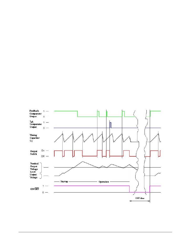
�Operating� Description�
�The� NCP3066� operates� as� a� fixed� oscillator� frequency�
�output� voltage� ripple� gated� regulator.� In� general,� this� mode�
�of� operation� is� somewhat� analogous� to� a� capacitor� charge�
�pump� and� does� not� require� dominant� pole� loop�
�compensation� for� converter� stability.� The� typical� operating�
�waveforms� are� shown� in� Figure� 12.� The� output� voltage�
�waveform� is� shown� for� a� step� ?� down� converter� with� the�
�ripple� and� phasing� exaggerated� for� clarity.� During� initial�
�converter� startup,� the� feedback� comparator� senses� that� the�
�output� voltage� level� is� below� nominal.� This� causes� the�
�output� switch� to� turn� on� and� off� at� a� frequency� and� duty� cycle�
�controlled� by� the� oscillator,� thus� pumping� up� the� output� filter�
�comparator� value,� the� output� switch� cycle� is� inhibited.� When�
�the� load� current� causes� the� output� voltage� to� fall� below� the�
�nominal� value� feedback� comparator� enables� switching�
�immediately.� Under� these� conditions,� the� output� switch�
�conduction� can� be� enabled� for� a� partial� oscillator� cycle,� a�
�partial� cycle� plus� a� complete� cycle,� multiple� cycles,� or� a�
�partial� cycle� plus� multiple� cycles.�
�Oscillator�
�The� oscillator� frequency� and� off� ?� time� of� the� output� switch�
�are� programmed� by� the� value� of� the� timing� capacitor� C� T� .� The�
�capacitor� C� T� is� charged� and� discharged� by� a� 1� to� 6� ratio�
�internal� current� source� and� sink,� generating� a� positive� going�
�sawtooth� waveform� at� Pin� 3.� This� ratio� sets� the� maximum�
�t� ON� /(t� ON� +� t� OFF� )� of� the� switching� converter� as� 6/(6+1)� or�
�85.7%� (typical).� The� oscillator� peak� and� valley� voltage�
�difference� is� 500� mV� typically.� To� calculate� the� C� T� capacitor�
�value� for� required� oscillator� frequency,� use� the� equations�
�found� in� Figure� 15.� An� online� NCP3066� design� tool� can� be�
�found� at� www.onsemi.com,� which� aids� in� selecting�
�component� values.�
�capacitor.� When� the� output� voltage� level� reaches� nominal�
�Figure� 12.� Typical� Operating� Waveforms�
�http://onsemi.com�
�7�
�相关PDF资料 |
PDF描述 |
|---|---|
| VLF4012AT-6R8MR96 | INDUCTOR POWER 6.8UH .96A SMD |
| P51-300-S-W-M12-4.5V-000-000 | SENSOR 300PSI 1/8-27NPT .5-4.5V |
| REC7.5-1209DRW/H1/A/M/SMD | CONV DC/DC 7.5W 9-18VIN +/-09V |
| REC3-243.3DRWZ/H2/A/M/SMD-R | CONV DC/DC 3W 9-36VIN +/-3.3VOUT |
| P51-15-S-UCF-P-5V-000-000 | SENSOR 15PSIS 9/16 UNF 5V |
相关代理商/技术参数 |
参数描述 |
|---|---|
| NCV3066MNTXG | 功能描述:直流/直流开关调节器 1.5A SW REG FOR LED WITH ENABLE RoHS:否 制造商:International Rectifier 最大输入电压:21 V 开关频率:1.5 MHz 输出电压:0.5 V to 0.86 V 输出电流:4 A 输出端数量: 最大工作温度: 安装风格:SMD/SMT 封装 / 箱体:PQFN 4 x 5 |
| NCV3066PG | 功能描述:直流/直流开关调节器 1.5A SW REG FOR LED WITH ENABLE RoHS:否 制造商:International Rectifier 最大输入电压:21 V 开关频率:1.5 MHz 输出电压:0.5 V to 0.86 V 输出电流:4 A 输出端数量: 最大工作温度: 安装风格:SMD/SMT 封装 / 箱体:PQFN 4 x 5 |
| NCV3163 | 制造商:ONSEMI 制造商全称:ON Semiconductor 功能描述:3.4 A, Step−Up/Down/Inverting 50−300 kHz Switching Regulator |
| NCV3163MNR2G | 功能描述:直流/直流开关转换器 3.4A STEP UP/DWN/INV RoHS:否 制造商:STMicroelectronics 最大输入电压:4.5 V 开关频率:1.5 MHz 输出电压:4.6 V 输出电流:250 mA 输出端数量:2 最大工作温度:+ 85 C 安装风格:SMD/SMT |
| NCV3163PWG | 功能描述:直流/直流开关转换器 3.4A STEP UP/DWN/INV RoHS:否 制造商:STMicroelectronics 最大输入电压:4.5 V 开关频率:1.5 MHz 输出电压:4.6 V 输出电流:250 mA 输出端数量:2 最大工作温度:+ 85 C 安装风格:SMD/SMT |
发布紧急采购,3分钟左右您将得到回复。