- 您现在的位置:买卖IC网 > PDF目录20813 > NCV3066DR2G (ON Semiconductor)IC LED DRIVER HIGH BRIGHT 8-SOIC PDF资料下载
参数资料
| 型号: | NCV3066DR2G |
| 厂商: | ON Semiconductor |
| 文件页数: | 9/20页 |
| 文件大小: | 0K |
| 描述: | IC LED DRIVER HIGH BRIGHT 8-SOIC |
| 标准包装: | 2,500 |
| 恒定电流: | 是 |
| 拓扑: | PWM,降压(降压),升压(升压) |
| 输出数: | 1 |
| 内部驱动器: | 是 |
| 类型 - 主要: | 车载 |
| 类型 - 次要: | 高亮度 LED(HBLED) |
| 频率: | 100kHz ~ 250kHz |
| 电源电压: | 3 V ~ 40 V |
| 安装类型: | 表面贴装 |
| 封装/外壳: | 8-SOIC(0.154",3.90mm 宽) |
| 供应商设备封装: | 8-SOICN |
| 包装: | 带卷 (TR) |
| 工作温度: | -40°C ~ 125°C |
�� �
�
�NCP3066,� NCV3066�
�APPLICATIONS�
�Figures� 15� through� 24� show� the� simplicity� and� flexibility�
�of� the� NCP3066.� Two� main� converter� topologies� are�
�demonstrated� with� actual� test� data� shown� below� each� of� the�
�circuit� diagrams.� The� demo� boards� have� an� input� for� a� digital�
�dimming� signal.� You� can� provide� a� PWM� signal� to� change�
�the� average� output� current� and� reduce� the� LED� brightness.�
�Figure� 14� gives� the� relevant� design� equations� for� the� key�
�parameters.� Additionally,� a� complete� application� design� aid�
�for� the� NCP3066� can� be� found� at� www.onsemi.com.�
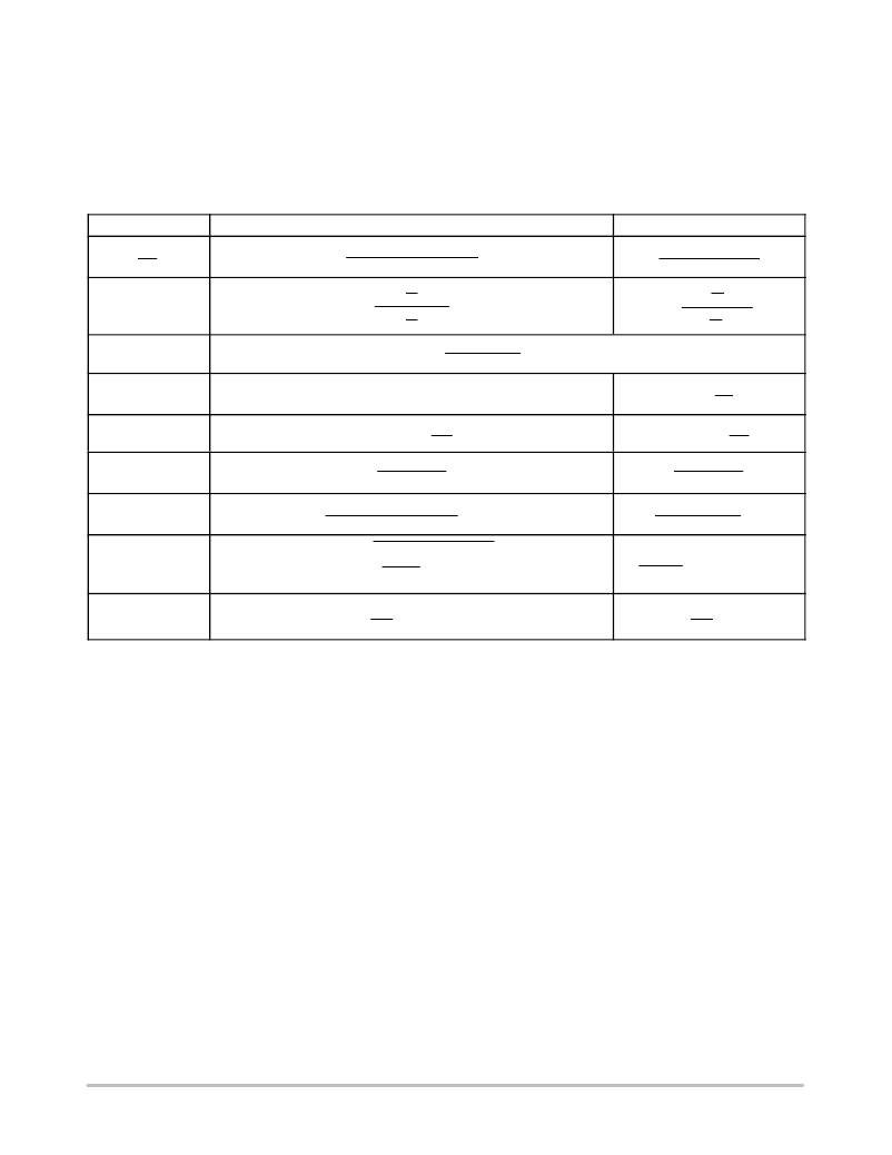
�Parameter�
�ton�
�toff�
�t� on�
�Step� ?� Down�
�Vout� )� VF�
�Vin� *� VSWCE� *� Vout�
�ton�
�toff�
�Step� ?� Up�
�Vout� )� VF� *� Vin�
�Vin� *� VSWCE�
�ton�
�toff�
�f�
�ton�
�toff�
�)� 1�
�f�
�ton�
�toff�
�)� 1�
�CT� +� 381.6� @� 10�
�C� T�
�f� osc�
�*� 6�
�*� 343�
�10� *� 12�
�I� L(avg)�
�Iout�
�Iout�
�ton�
�toff�
�)� 1�
�I� pk� (Switch)�
�IL(avg)� )�
�D� IL�
�2�
�IL(avg)� )�
�D� IL�
�2�
�R� SC�
�0.20�
�Ipk� (Switch)�
�0.20�
�Ipk� (Switch)�
�L�
�Vin� *� VSWCE� *� Vout�
�D� IL�
�ton�
�Vin� *� VSWCE�
�D� IL�
�ton�
�V� ripple(pp)�
�D� IL�
�1�
�8� f� CO�
�2�
�)� (ESR)� 2�
�ton Iout�
�CO�
�)� D� IL�
�ESR�
�I� out�
�V� ref�
�R� s�
�V� ref�
�R� s�
�9.� V� SWCE� ?� Darlington� Switch� Collector� to� Emitter� Voltage� Drop,� refer� to� Figures� 7� and� 8.�
�10.� V� F� ?� Output� rectifier� forward� voltage� drop.� Typical� value� for� 1N5819� Schottky� barrier� rectifier� is� 0.4� V.�
�11.� The� calculated� t� on� /t� off� must� not� exceed� the� minimum� guaranteed� oscillator� charge� to� discharge� ratio.�
�Figure� 14.� Design� Equations�
�The� Following� Converter� Characteristics� Must� Be� Chosen:�
�V� in� ?� Nominal� operating� input� voltage.�
�V� out� ?� Desired� output� voltage.�
�I� out� ?� Desired� output� current.�
�D� I� L� ?� Desired� peak� ?� to� ?� peak� inductor� ripple� current.� For� maximum� output� current� it� is� suggested� that� D� I� L� be� chosen� to� be�
�less� than� 10%� of� the� average� inductor� current� I� L(avg)� .� This� will� help� prevent� I� pk� (Switch)� from� reaching� the� current� limit� threshold�
�set� by� R� SC� .� If� the� design� goal� is� to� use� a� minimum� inductance� value,� let� D� I� L� =� 2(I� L(avg)� ).� This� will� proportionally� reduce�
�converter� output� current� capability.�
�f� ?� Maximum� output� switch� frequency.�
�V� ripple(pp)� ?� Desired� peak� ?� to� ?� peak� output� ripple� voltage.� For� best� performance� the� ripple� voltage� should� be� kept� to� a� low�
�value� since� it� will� directly� affect� line� and� load� regulation.� Capacitor� C� O� should� be� a� low� equivalent� series� resistance� (ESR)�
�electrolytic� designed� for� switching� regulator� applications.�
�http://onsemi.com�
�9�
�相关PDF资料 |
PDF描述 |
|---|---|
| VLF4012AT-6R8MR96 | INDUCTOR POWER 6.8UH .96A SMD |
| P51-300-S-W-M12-4.5V-000-000 | SENSOR 300PSI 1/8-27NPT .5-4.5V |
| REC7.5-1209DRW/H1/A/M/SMD | CONV DC/DC 7.5W 9-18VIN +/-09V |
| REC3-243.3DRWZ/H2/A/M/SMD-R | CONV DC/DC 3W 9-36VIN +/-3.3VOUT |
| P51-15-S-UCF-P-5V-000-000 | SENSOR 15PSIS 9/16 UNF 5V |
相关代理商/技术参数 |
参数描述 |
|---|---|
| NCV3066MNTXG | 功能描述:直流/直流开关调节器 1.5A SW REG FOR LED WITH ENABLE RoHS:否 制造商:International Rectifier 最大输入电压:21 V 开关频率:1.5 MHz 输出电压:0.5 V to 0.86 V 输出电流:4 A 输出端数量: 最大工作温度: 安装风格:SMD/SMT 封装 / 箱体:PQFN 4 x 5 |
| NCV3066PG | 功能描述:直流/直流开关调节器 1.5A SW REG FOR LED WITH ENABLE RoHS:否 制造商:International Rectifier 最大输入电压:21 V 开关频率:1.5 MHz 输出电压:0.5 V to 0.86 V 输出电流:4 A 输出端数量: 最大工作温度: 安装风格:SMD/SMT 封装 / 箱体:PQFN 4 x 5 |
| NCV3163 | 制造商:ONSEMI 制造商全称:ON Semiconductor 功能描述:3.4 A, Step−Up/Down/Inverting 50−300 kHz Switching Regulator |
| NCV3163MNR2G | 功能描述:直流/直流开关转换器 3.4A STEP UP/DWN/INV RoHS:否 制造商:STMicroelectronics 最大输入电压:4.5 V 开关频率:1.5 MHz 输出电压:4.6 V 输出电流:250 mA 输出端数量:2 最大工作温度:+ 85 C 安装风格:SMD/SMT |
| NCV3163PWG | 功能描述:直流/直流开关转换器 3.4A STEP UP/DWN/INV RoHS:否 制造商:STMicroelectronics 最大输入电压:4.5 V 开关频率:1.5 MHz 输出电压:4.6 V 输出电流:250 mA 输出端数量:2 最大工作温度:+ 85 C 安装风格:SMD/SMT |
发布紧急采购,3分钟左右您将得到回复。