参数资料
| 型号: | NCV7356D1R2G |
| 厂商: | ON Semiconductor |
| 文件页数: | 3/24页 |
| 文件大小: | 0K |
| 描述: | IC TXRX CAN SGL WIRE 8-SOIC |
| 标准包装: | 1 |
| 类型: | 收发器 |
| 驱动器/接收器数: | 1/1 |
| 规程: | CAN |
| 电源电压: | 5 V ~ 27 V |
| 安装类型: | 表面贴装 |
| 封装/外壳: | 8-SOIC(0.154",3.90mm 宽) |
| 供应商设备封装: | 8-SOICN |
| 包装: | 标准包装 |
| 其它名称: | NCV7356D1R2GOSDKR |
NCV7356
http://onsemi.com
11
FUNCTIONAL DESCRIPTION
TxD Input Pin
TxD Polarity
TxD = logic 1 (or floating) on this pin produces an
undriven or recessive bus state (low bus voltage)
TxD = logic 0 on this pin produces either a bus normal
or a bus high voltage dominant state depending on the
transceiver mode state (high bus voltage)
If the TxD pin is driven to a logic low state while the sleep
mode (Mode 0 = 0 and Mode 1 = 0) is activated, the
transceiver can not drive the CANH pin to the dominant
state.
The transceiver provides an internal pullup current on the
TxD pin which will cause the transmitter to default to the
bus recessive state when TxD is not driven.
TxD input signals are standard CMOS logic levels.
Timeout Feature
In case of a faulty blocked dominant TxD input signal,
the CANH output is switched off automatically after the
specified TxD timeout reaction time to prevent a dominant
bus.
The transmission is continued by next TxD L to H
transition without delay.
MODE0 and MODE1 Pins
The transceiver provides a weak internal pulldown
current on each of these pins which causes the transceiver
to default to sleep mode when they are not driven. The
mode input signals are standard CMOS logic level for
3.3 V and 5 V supply voltages. See Electrical
Characteristics table for timing limitations for mode
changes.
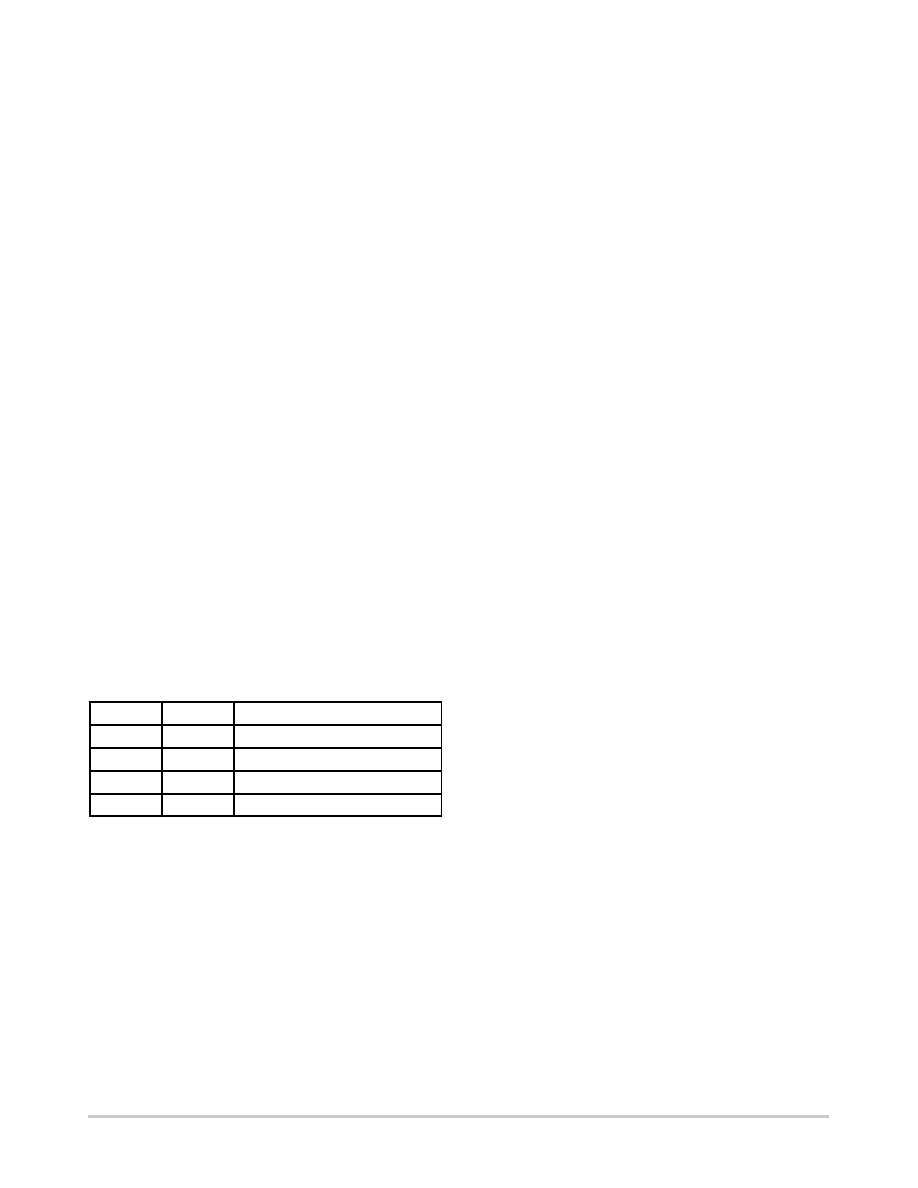
MODE0
MODE1
Mode
L
Sleep Mode
H
L
HighSpeed Mode
L
H
High Voltage WakeUp
H
Normal Mode
Sleep Mode
Transceiver is in low power state, waiting for wakeup
via high voltage signal or by mode pins change to any state
other than 0,0. In this state, the CANH pin is not in the
dominant state regardless of the state of the TxD pin.
HighSpeed Mode
This mode allows highspeed download with bit rates up
to 100 Kbit/s. The output wave shapingaping circuit is
disabled in this mode. Bus transmitter drive circuits for
those nodes which are required to communicate in
highspeed mode are able to drive reduced bus resistance
in this mode.
High Voltage WakeUp Mode
This bus includes a selective node awake capability,
which allows normal communication to take place among
some nodes while leaving the other nodes in an undisturbed
sleep state. This is accomplished by controlling the signal
voltages such that all nodes must wakeup when they
receive a higher voltage message signal waveform. The
communication system communicates to the nodes
information as to which nodes are to stay operational
(awake) and which nodes are to put themselves into a non
communicating low power “sleep” state. Communication
at the lower, normal voltage levels shall not disturb the
sleeping nodes.
Normal Mode
Transmission bit rate in normal communication is
33 Kbits/s. In normal transmission mode the NCV7356
supports controlled waveform rise and overshoot times.
Waveform trailing edge control is required to assure that
high frequency components are minimized at the
beginning of the downward voltage slope. The remaining
fall time occurs after the bus is inactive with drivers off and
is determined by the RC time constant of the total bus load.
RxD Output Pin
Logic data as sensed on the single wire CAN bus.
RxD Polarity
RxD = logic 1 on this pin indicates a bus recessive
state (low bus voltage)
RxD = logic 0 on this pin indicates a bus normal or
high voltage bus dominant state
RxD in Sleep Mode
RxD does not pass signals to the microprocessor while in
sleep mode until a valid wakeup bus voltage level is
received or the MODE0 and MODE 1 pins are not 0, 0
respectively. When the valid wakeup bus voltage signal
awakens the transceiver, the RxD pin signals an interrupt
(logic 0). If there is no mode change within 250 ms (typ),
the transceiver reenters the sleep mode.
When not in sleep mode all valid bus signals will be sent
out on the RxD pin.
RxD will be placed in the undriven or off state when in
sleep mode.
RxD Typical Load
Resistance: 2.7 k
W
Capacitance: < 25 pF
相关PDF资料 |
PDF描述 |
|---|---|
| MAX166DCWP+ | IC ADC 8BIT MPU COMP 20-SOIC |
| IDT72V295L20PF8 | IC FIFO SUPERSYNCII 20NS 64-TQFP |
| CS3108A-12S-1S | CONN PLUG 2POS RT ANG W/SCKT |
| IDT72V295L15PF8 | IC FIFO SUPERSYNCII 15NS 64-TQFP |
| MS3101F22-9S | CONN RCPT 3POS FREE HNG W/SCKT |
相关代理商/技术参数 |
参数描述 |
|---|---|
| NCV7356D2 | 功能描述:网络控制器与处理器 IC Single Wire CAN RoHS:否 制造商:Micrel 产品:Controller Area Network (CAN) 收发器数量: 数据速率: 电源电流(最大值):595 mA 最大工作温度:+ 85 C 安装风格:SMD/SMT 封装 / 箱体:PBGA-400 封装:Tray |
| NCV7356D2G | 功能描述:网络控制器与处理器 IC SINGLE WIRE CAN RoHS:否 制造商:Micrel 产品:Controller Area Network (CAN) 收发器数量: 数据速率: 电源电流(最大值):595 mA 最大工作温度:+ 85 C 安装风格:SMD/SMT 封装 / 箱体:PBGA-400 封装:Tray |
| NCV7356D2R2 | 功能描述:网络控制器与处理器 IC Single Wire CAN RoHS:否 制造商:Micrel 产品:Controller Area Network (CAN) 收发器数量: 数据速率: 电源电流(最大值):595 mA 最大工作温度:+ 85 C 安装风格:SMD/SMT 封装 / 箱体:PBGA-400 封装:Tray |
| NCV7356D2R2G | 功能描述:网络控制器与处理器 IC SINGLE WIRE CAN RoHS:否 制造商:Micrel 产品:Controller Area Network (CAN) 收发器数量: 数据速率: 电源电流(最大值):595 mA 最大工作温度:+ 85 C 安装风格:SMD/SMT 封装 / 箱体:PBGA-400 封装:Tray |
| NCV7356DR2 | 制造商:ONSEMI 制造商全称:ON Semiconductor 功能描述:Single Wire CAN Transceiver |
发布紧急采购,3分钟左右您将得到回复。