- 您现在的位置:买卖IC网 > PDF目录10245 > NE570DG (ON Semiconductor)IC COMPANDOR DUAL GAIN 16-SOIC PDF资料下载
参数资料
| 型号: | NE570DG |
| 厂商: | ON Semiconductor |
| 文件页数: | 4/10页 |
| 文件大小: | 0K |
| 描述: | IC COMPANDOR DUAL GAIN 16-SOIC |
| 标准包装: | 47 |
| 类型: | 压缩扩展器 |
| 应用: | 蜂窝式无线电,播放器 |
| 安装类型: | 表面贴装 |
| 封装/外壳: | 16-SOIC(0.295",7.50mm 宽) |
| 供应商设备封装: | 16-SOIC W |
| 包装: | 管件 |
| 其它名称: | NE570DG-ND NE570DGOS |
NE570
http://onsemi.com
3
CIRCUIT DESCRIPTION
The NE570 compandor building blocks, as shown in the
block diagram, are a fullwave rectifier, a variable gain cell,
an operational amplifier and a bias system. The arrangement
of these blocks in the IC result in a circuit which can perform
well with few external components, yet can be adapted to
many diverse applications.
The fullwave rectifier rectifies the input current which
flows from the rectifier input, to an internal summing node
which is biased at VREF. The rectified current is averaged on
an external filter capacitor tied to the CRECT terminal, and
the average value of the input current controls the gain of the
variable gain cell. The gain will thus be proportional to the
average value of the input signal for capacitivelycoupled
voltage inputs as shown in the following equation. Note that
for capacitivelycoupled inputs there is no offset voltage
capable of producing a gain error. The only error will come
from the bias current of the rectifier (supplied internally)
which is less than 0.1
mA.
G
T
|V
IN * VREF |avg
R
1
or
G
T
|V
IN |avg
R
1
The speed with which gain changes to follow changes in
input signal levels is determined by the rectifier filter
capacitor. A small capacitor will yield rapid response but
will not fully filter low frequency signals. Any ripple on the
gain control signal will modulate the signal passing through
the variable gain cell. In an expander or compressor
application, this would lead to third harmonic distortion, so
there is a tradeoff to be made between fast attack and decay
times and distortion. For step changes in amplitude, the
change in gain with time is shown by this equation.
t + 10kW
C
RECT
G(t)
+ (G
initial * Gfinal)e
*t
t
) G
final
The variable gain cell is a currentin, currentout device
with the ratio IOUT/IIN controlled by the rectifier. IIN is the
current which flows from the
DG input to an internal
summing node biased at VREF. The following equation
applies for capacitivelycoupled inputs. The output current,
IOUT, is fed to the summing node of the op amp.
I
IN +
V
IN * VREF
R
2
+
V
IN
R
2
A compensation scheme built into the
DG cell
compensates for temperature and cancels out odd harmonic
distortion. The only distortion which remains is even
harmonics, and they exist only because of internal offset
voltages. The THD trim terminal provides a means for
nulling the internal offsets for low distortion operation.
The
operational
amplifier
(which
is
internally
compensated) has the noninverting input tied to VREF, and
the inverting input connected to the
DG cell output as well
as brought out externally. A resistor, R3, is brought out from
the summing node and allows compressor or expander gain
to be determined only by internal components.
The output stage is capable of
±20 mA output current.
This allows a +13 dBm (3.5 VRMS) output into a 300 W load
which, with a series resistor and proper transformer, can
result in +13 dBm with a 600
W output impedance.
A bandgap reference provides the reference voltage for all
summing nodes, a regulated supply voltage for the rectifier
and
DG cell, and a bias current for the DG cell. The low
tempco of this type of reference provides very stable biasing
over a wide temperature range.
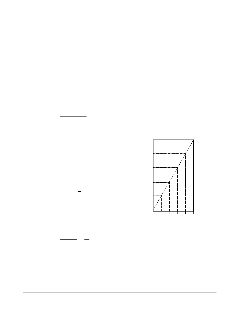
The typical performance characteristics illustration
shows the basic inputoutput transfer curve for basic
compressor or expander circuits.
+20
+10
0
10
20
30
40
50
60
70
80
40
30 20 10
0
+10
COMPRESSOR OUTPUT LEVEL
OR
EXPANDOR INPUT LEVEL (dBm)
COMPRESSOR
INPUT
LEVEL
OR
EXP
ANDOR
OUTPUT
LEVEL
(dBm)
Figure 2. Basic InputOutput Transfer Curve
相关PDF资料 |
PDF描述 |
|---|---|
| MS27473E10A35PB | CONN PLUG 13POS STRAIGHT W/PINS |
| LTC2391CUK-16#PBF | IC ADC 16BIT SER/PAR 250K 48QFN |
| LTC1418IG#TR | IC A/D CONV 14BIT SRL&PAR 28SSOP |
| MS3106F24-9P | CONN PLUG 2POS STRAIGHT W/PINS |
| LTC2351HUH-12#PBF | IC ADC 12BIT 1.5MSPS 32-QFN |
相关代理商/技术参数 |
参数描述 |
|---|---|
| NE570DR2 | 功能描述:通信集成电路 - 若干 Dual Gain Compandor RoHS:否 制造商:Maxim Integrated 类型:Transport Devices 封装 / 箱体:TECSBGA-256 数据速率:100 Mbps 电源电压-最大:1.89 V, 3.465 V 电源电压-最小:1.71 V, 3.135 V 电源电流:50 mA, 225 mA 最大工作温度:+ 85 C 最小工作温度:- 40 C 封装:Tube |
| NE570DR2G | 功能描述:通信集成电路 - 若干 Dual Gain Compandor Commercial Temp RoHS:否 制造商:Maxim Integrated 类型:Transport Devices 封装 / 箱体:TECSBGA-256 数据速率:100 Mbps 电源电压-最大:1.89 V, 3.465 V 电源电压-最小:1.71 V, 3.135 V 电源电流:50 mA, 225 mA 最大工作温度:+ 85 C 最小工作温度:- 40 C 封装:Tube |
| NE570D-T | 制造商:未知厂家 制造商全称:未知厂家 功能描述:Compander |
| NE570F | 制造商:未知厂家 制造商全称:未知厂家 功能描述:Analog Miscellaneous |
| NE570N | 制造商:NXP Semiconductors 功能描述: |
发布紧急采购,3分钟左右您将得到回复。