- 您现在的位置:买卖IC网 > PDF目录10245 > NE570DG (ON Semiconductor)IC COMPANDOR DUAL GAIN 16-SOIC PDF资料下载
参数资料
| 型号: | NE570DG |
| 厂商: | ON Semiconductor |
| 文件页数: | 5/10页 |
| 文件大小: | 0K |
| 描述: | IC COMPANDOR DUAL GAIN 16-SOIC |
| 标准包装: | 47 |
| 类型: | 压缩扩展器 |
| 应用: | 蜂窝式无线电,播放器 |
| 安装类型: | 表面贴装 |
| 封装/外壳: | 16-SOIC(0.295",7.50mm 宽) |
| 供应商设备封装: | 16-SOIC W |
| 包装: | 管件 |
| 其它名称: | NE570DG-ND NE570DGOS |
NE570
http://onsemi.com
4
13
2, 15
4
1, 16
5, 12
8, 9
7, 10
6, 11
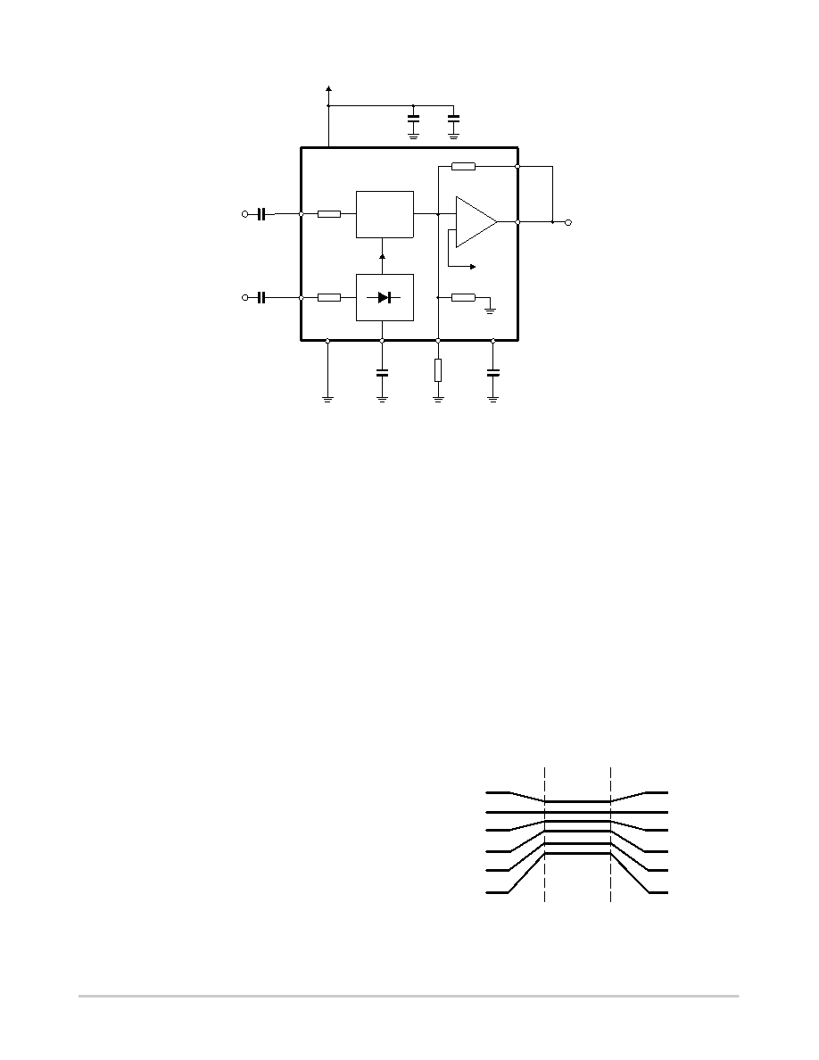
V1
V2
VO
VCC = 15 V
VREF
10
mF
0.1
mF
200 pF
8.2 k
W
2.2
mF
+
30 k
W
20 k
W
DG
10 k
W
20 k
W
2.2
mF
3, 14
2.2
mF
Figure 3. Typical Test Circuit
INTRODUCTION
Much interest has been expressed in high performance
electronic gain control circuits. For noncritical applications,
an integrated circuit operational transconductance amplifier
can be used, but when highperformance is required, one has
to resort to complex discrete circuitry with many expensive,
wellmatched
components.
This paper
describes an
inexpensive integrated circuit, the NE570 Compandor, which
offers a pair of high performance gain control circuits
featuring low distortion (<0.1 %), high signaltonoise ratio
(90 dB), and wide dynamic range (110 dB).
CIRCUIT BACKGROUND
The NE570 Compandor was originally designed to satisfy
the requirements of the telephone system. When several
telephone channels are multiplexed onto a common line, the
resulting signaltonoise ratio is poor and companding is
used to allow a wider dynamic range to be passed through the
channel. Figure 4 graphically shows what a compandor can
do for the signaltonoise ratio of a restricted dynamic range
channel. The input level range of +20 dB to 80 dB is shown
undergoing a 2to1 compression where a 2.0 dB input level
change is compressed into a 1.0 dB output level change by the
compressor. The original 100 dB of dynamic range is thus
compressed to a 50 dB range for transmission through a
restricted dynamic range channel. A complementary
expansion on the receiving end restores the original signal
levels and reduces the channel noise by as much as 45 dB.
The significant circuits in a compressor or expander are
the rectifier and the gain control element. The phone system
requires a simple fullwave averaging rectifier with good
accuracy, since the rectifier accuracy determines the (input)
output level tracking accuracy. The gain cell determines the
distortion and noise characteristics, and the phone system
specifications here are very loose. These specs could have
been met with a simple operational transconductance
multiplier, or OTA, but the gain of an OTA is proportional
to temperature and this is very undesirable. Therefore, a
linearized transconductance multiplier was designed which
is insensitive to temperature and offers low noise and low
distortion performance. These features make the circuit
useful in audio and data systems as well as in
telecommunications systems.
INPUT
LEVEL
COMPRESSION
EXP
ANSION
OUTPUT
LEVEL
NOISE
+20
0 dB
40
80
20
0 dB
40
80
Figure 4. Restricted Dynamic Range Channel
相关PDF资料 |
PDF描述 |
|---|---|
| MS27473E10A35PB | CONN PLUG 13POS STRAIGHT W/PINS |
| LTC2391CUK-16#PBF | IC ADC 16BIT SER/PAR 250K 48QFN |
| LTC1418IG#TR | IC A/D CONV 14BIT SRL&PAR 28SSOP |
| MS3106F24-9P | CONN PLUG 2POS STRAIGHT W/PINS |
| LTC2351HUH-12#PBF | IC ADC 12BIT 1.5MSPS 32-QFN |
相关代理商/技术参数 |
参数描述 |
|---|---|
| NE570DR2 | 功能描述:通信集成电路 - 若干 Dual Gain Compandor RoHS:否 制造商:Maxim Integrated 类型:Transport Devices 封装 / 箱体:TECSBGA-256 数据速率:100 Mbps 电源电压-最大:1.89 V, 3.465 V 电源电压-最小:1.71 V, 3.135 V 电源电流:50 mA, 225 mA 最大工作温度:+ 85 C 最小工作温度:- 40 C 封装:Tube |
| NE570DR2G | 功能描述:通信集成电路 - 若干 Dual Gain Compandor Commercial Temp RoHS:否 制造商:Maxim Integrated 类型:Transport Devices 封装 / 箱体:TECSBGA-256 数据速率:100 Mbps 电源电压-最大:1.89 V, 3.465 V 电源电压-最小:1.71 V, 3.135 V 电源电流:50 mA, 225 mA 最大工作温度:+ 85 C 最小工作温度:- 40 C 封装:Tube |
| NE570D-T | 制造商:未知厂家 制造商全称:未知厂家 功能描述:Compander |
| NE570F | 制造商:未知厂家 制造商全称:未知厂家 功能描述:Analog Miscellaneous |
| NE570N | 制造商:NXP Semiconductors 功能描述: |
发布紧急采购,3分钟左右您将得到回复。