- 您现在的位置:买卖IC网 > PDF目录10245 > NE570DG (ON Semiconductor)IC COMPANDOR DUAL GAIN 16-SOIC PDF资料下载
参数资料
| 型号: | NE570DG |
| 厂商: | ON Semiconductor |
| 文件页数: | 9/10页 |
| 文件大小: | 0K |
| 描述: | IC COMPANDOR DUAL GAIN 16-SOIC |
| 标准包装: | 47 |
| 类型: | 压缩扩展器 |
| 应用: | 蜂窝式无线电,播放器 |
| 安装类型: | 表面贴装 |
| 封装/外壳: | 16-SOIC(0.295",7.50mm 宽) |
| 供应商设备封装: | 16-SOIC W |
| 包装: | 管件 |
| 其它名称: | NE570DG-ND NE570DGOS |
NE570
http://onsemi.com
8
this, which means our overall offsets are typically about mV.
The distortion is not affected by the magnitude of the gain
control current, and it does not increase as the gain is
changed. This second harmonic distortion could be
eliminated by making perfect transistors, but since that
would be difficult, we have had to resort to other methods.
A trim pin has been provided to allow trimming of the
internal offsets to zero, which effectively eliminated second
harmonic distortion. Figure 14 shows the simple trim
network required.
3.6 V
VCC
R
20 k
W
6.2 k
W
To THD Trim
≈200 pF
Figure 14. THD Trim Network
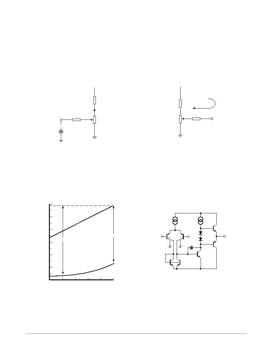
Figure 15 shows the noise performance of the
DG cell. The
maximum output level before clipping occurs in the gain cell
is plotted along with the output noise in a 20 kHz bandwidth.
Note that the noise drops as the gain is reduced for the first
20 dB of gain reduction. At high gains, the signal to noise
ratio is 90 dB, and the total dynamic range from maximum
signal to minimum noise is 110 dB.
VCA GAIN (dB)
+20
OUTPUT
(dBm)
0
20
40
60
80
100
40
20
0
MAXIMUM
SIGNAL LEVEL
NOISE IN
20 kHz BW
90 dB
110 dB
Figure 15. Dynamic Range
Control signal feedthrough is generated in the gain cell by
imperfect device matching and mismatches in the current
sources, I1 and I2. When no input signal is present, changing
IG will cause a small output signal. The distortion trim is
effective in nulling out any control signal feedthrough, but
in general, the null for minimum feedthrough will be
different than the null in distortion. The control signal
feedthrough can be trimmed independently of distortion by
tying a current source to the
DG input pin. This effectively
RSELECT FOR
3.6 V
470 k
W
TO PIN 3 OR 14
100 k
W
VCC
Figure 16. Control Signal Feedthrough
OPERATIONAL AMPLIFIER
The main op amp shown in the chip block diagram is
equivalent to a 741 with a 1.0 MHz bandwidth. Figure 17
shows the basic circuit. Split collectors are used in the input
pair to reduce gM, so that a small compensation capacitor of
just 10 pF may be used. The output stage, although capable
of output currents in excess of 20 mA, is biased for a low
quiescent current to conserve power. When driving heavy
loads, this leads to a small amount of crossover distortion.
OUT
Q5
I1
I2
Q1
D2
IN
+IN
Q2
Q3
Q4
CC
D1
Q6
Figure 17. Operational Amplifier
相关PDF资料 |
PDF描述 |
|---|---|
| MS27473E10A35PB | CONN PLUG 13POS STRAIGHT W/PINS |
| LTC2391CUK-16#PBF | IC ADC 16BIT SER/PAR 250K 48QFN |
| LTC1418IG#TR | IC A/D CONV 14BIT SRL&PAR 28SSOP |
| MS3106F24-9P | CONN PLUG 2POS STRAIGHT W/PINS |
| LTC2351HUH-12#PBF | IC ADC 12BIT 1.5MSPS 32-QFN |
相关代理商/技术参数 |
参数描述 |
|---|---|
| NE570DR2 | 功能描述:通信集成电路 - 若干 Dual Gain Compandor RoHS:否 制造商:Maxim Integrated 类型:Transport Devices 封装 / 箱体:TECSBGA-256 数据速率:100 Mbps 电源电压-最大:1.89 V, 3.465 V 电源电压-最小:1.71 V, 3.135 V 电源电流:50 mA, 225 mA 最大工作温度:+ 85 C 最小工作温度:- 40 C 封装:Tube |
| NE570DR2G | 功能描述:通信集成电路 - 若干 Dual Gain Compandor Commercial Temp RoHS:否 制造商:Maxim Integrated 类型:Transport Devices 封装 / 箱体:TECSBGA-256 数据速率:100 Mbps 电源电压-最大:1.89 V, 3.465 V 电源电压-最小:1.71 V, 3.135 V 电源电流:50 mA, 225 mA 最大工作温度:+ 85 C 最小工作温度:- 40 C 封装:Tube |
| NE570D-T | 制造商:未知厂家 制造商全称:未知厂家 功能描述:Compander |
| NE570F | 制造商:未知厂家 制造商全称:未知厂家 功能描述:Analog Miscellaneous |
| NE570N | 制造商:NXP Semiconductors 功能描述: |
发布紧急采购,3分钟左右您将得到回复。