参数资料
| 型号: | NE570DR2 |
| 厂商: | ON Semiconductor |
| 文件页数: | 6/10页 |
| 文件大小: | 0K |
| 描述: | IC COMPANDOR DUAL GAIN 16-SOIC |
| 标准包装: | 1,000 |
| 类型: | 压缩扩展器 |
| 应用: | 蜂窝式无线电,播放器 |
| 安装类型: | 表面贴装 |
| 封装/外壳: | 16-SOIC(0.295",7.50mm 宽) |
| 供应商设备封装: | 16-SOIC W |
| 包装: | 带卷 (TR) |
NE570
http://onsemi.com
5
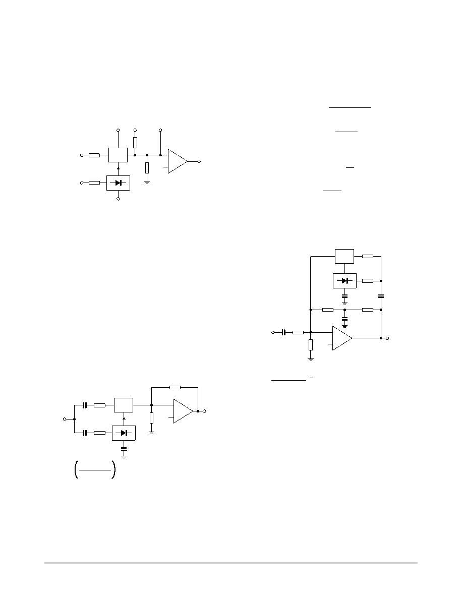
BASIC CIRCUIT HOOKUP AND OPERATION
Figure 5 shows the block diagram of one half of the chip,
(there are two identical channels on the IC). The fullwave
averaging rectifier provides a gain control current, IG, for the
variable gain (
DG) cell. The output of theDG cell is a current
which is fed to the summing node of the operational
amplifier. Resistors are provided to establish circuit gain and
set the output DC bias.
7, 10
OUTPUT
+
DG
R2
20 k
W
VREF
1.8 V
5, 12
INV. IN
R3
6, 11
R3
20 k
W
R4
30 k
W
VCC: PIN 13
GND: PIN 4
IG
CRECT
1, 16
8, 9
THD_TRIM
R1
10 k
W
RECT_IN
2, 15
3, 14
DG_CELL_IN
Figure 5. Chip Block Diagram (1 of 2 Channels)
The circuit is intended for use in single power supply
systems, so the internal summing nodes must be biased at
some voltage above ground. An internal band gap voltage
reference provides a very stable, low noise 1.8 V reference
denoted VREF. The noninverting input of the op amp is tied
to VREF, and the summing nodes of the rectifier and DG cell
(located at the right of R1 and R2) have the same potential.
The THD_TRIM pin is also at the VREF potential.
Figure 6 shows how the circuit is hooked up to realize an
expander. The input signal, VIN, is applied to the inputs of
both the rectifier and the
DG cell. When the input signal
drops by 6.0 dB, the gain control current will drop by a factor
of 2, and so the gain will drop 6 dB. The output level at VOUT
will thus drop 12 dB, giving us the desired 2to1
expansion.
VOUT
+
DG
R4
VREF
R3
*CRECT
R2
R1
VIN
*CIN1
*CIN2
* EXTERNAL COMPONENTS
GAIN =
2 R3 VIN (Avg.)
R1 R2 IB
IB = 140 mA
NOTES:
Figure 6. Basic Expander
2
Figure 7 shows the hookup for a compressor. This is
essentially an expander placed in the feedback loop of the op
amp. The
DG cell is setup to provide AC feedback only, so
a separate DC feedback loop is provided by the two RDC and
CDC. The values of RDC will determine the DC bias at the
output of the op amp. The output will bias to:
V
OUT DC +
1
)
R
DC1 ) RDC2
R
4
V
REF
V
OUT DC +
1
)
R
DC TOT
30 k
W
1.8 V
The output of the expander will bias up to:
V
OUT DC +
1
)
R
3
R
4
V
REF
V
OUT DC +
1
) 20 kW
30 k
W
1.8 V
+ 3.0 V
The output will bias to 3.0 V when the internal resistors
are used. External resistors may be placed in series with R3,
(which will affect the gain), or in parallel with R4 to raise the
DC bias to any desired value.
VOUT
+
DG
R4
VREF
*RDC
*CDC
R3
VIN
*CIN
* EXTERNAL COMPONENTS
GAIN =
IB = 140 mA
NOTES:
*RDC
*CRECT
R1
R2
*CF
Figure 7. Basic Compressor
R1 R2 IB
2R3 VIN(avg.)
1
2
相关PDF资料 |
PDF描述 |
|---|---|
| NE592N14G | IC AMP VIDEO 2STAGE DIFF 14-DIP |
| NL17SH00P5T5G | SINGLE 2-INPUT NAND GATE SOT953 |
| NL17SH04P5T5G | IC GATE INVERTER SGL HS SOT953 |
| NL17SH08P5T5G | SINGLE 2-INPUT NAND GATE SOT953 |
| NL17SH32P5T5G | SINGLE 2-INPUT NAND GATE SOT953 |
相关代理商/技术参数 |
参数描述 |
|---|---|
| NE570DR2G | 功能描述:通信集成电路 - 若干 Dual Gain Compandor Commercial Temp RoHS:否 制造商:Maxim Integrated 类型:Transport Devices 封装 / 箱体:TECSBGA-256 数据速率:100 Mbps 电源电压-最大:1.89 V, 3.465 V 电源电压-最小:1.71 V, 3.135 V 电源电流:50 mA, 225 mA 最大工作温度:+ 85 C 最小工作温度:- 40 C 封装:Tube |
| NE570D-T | 制造商:未知厂家 制造商全称:未知厂家 功能描述:Compander |
| NE570F | 制造商:未知厂家 制造商全称:未知厂家 功能描述:Analog Miscellaneous |
| NE570N | 制造商:NXP Semiconductors 功能描述: |
| NE570N-B | 制造商:未知厂家 制造商全称:未知厂家 功能描述:Compander |
发布紧急采购,3分钟左右您将得到回复。