参数资料
| 型号: | NE570DR2 |
| 厂商: | ON Semiconductor |
| 文件页数: | 7/10页 |
| 文件大小: | 0K |
| 描述: | IC COMPANDOR DUAL GAIN 16-SOIC |
| 标准包装: | 1,000 |
| 类型: | 压缩扩展器 |
| 应用: | 蜂窝式无线电,播放器 |
| 安装类型: | 表面贴装 |
| 封装/外壳: | 16-SOIC(0.295",7.50mm 宽) |
| 供应商设备封装: | 16-SOIC W |
| 包装: | 带卷 (TR) |
NE570
http://onsemi.com
6
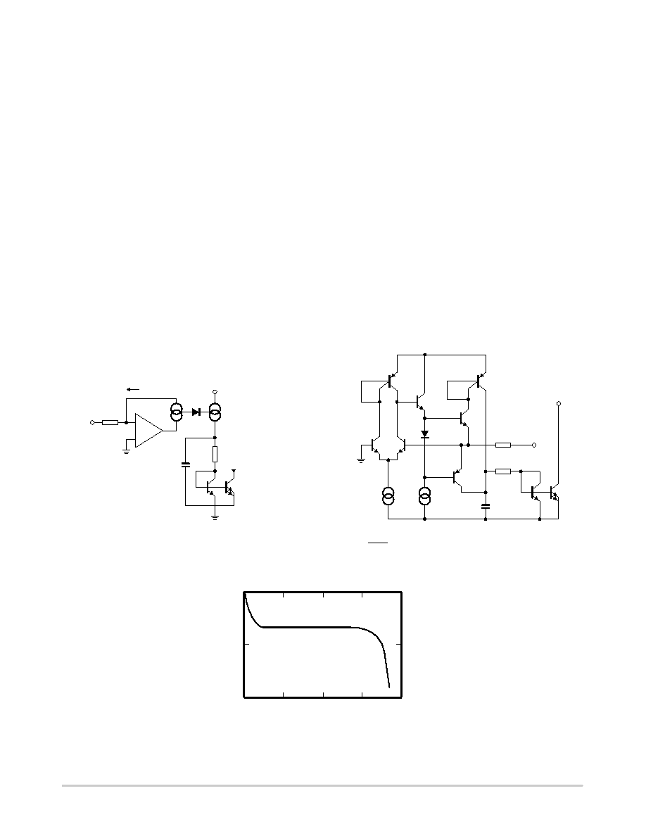
CIRCUIT DETAILSRECTIFIER
Figure 8 shows the concept behind the fullwave
averaging rectifier. The input current to the summing node
of the op amp, VIN/R1, is supplied by the output of the op
amp. If we can mirror the op amp output current into a
unipolar current, we will have an ideal rectifier. The output
current is averaged by R5, CR, which set the averaging time
constant, and then mirrored with a gain of 2 to become IG,
the gain control current.
Figure 9 shows the rectifier circuit in more detail. The op
amp is a onestage op amp, biased so that only one output
device is on at a time. The noninverting input, (the base of
Q1), which is shown grounded, is actually tied to the internal
1.8 V VREF. The inverting input is tied to the op amp output,
(the emitters of Q5 and Q6), and the input summing resistor
R1. The single diode between the bases of Q5 and Q6 assures
that only one device is on at a time. To detect the output
current of the op amp, we simply use the collector currents of
the output devices Q5 and Q6. Q6 will conduct when the
input swings positive and Q5 conducts when the input
swings negative. The collector currents will be in error by the
α of Q5 or Q6 on negative or positive signal swings,
respectively. ICs such as this have typical NPN
β’s of 200
and PNP
β’s of 40. The α’s of 0.995 and 0.975 will produce
errors of 0.5% on negative swings and 2.5% on positive
swings. The 1.5% average of these errors yields a mere
0.13 dB gain error.
At very low input signal levels the bias current of Q2,
(typically 50 nA), will become significant as it must be
supplied by Q5. Another low level error can be caused by DC
coupling into the rectifier. If an offset voltage exists between
the VIN input pin and the base of Q2, an error current of
VOS/R1 will be generated. A mere 1.0 mV of offset will
cause an input current of 100 nA, which will produce twice
the error of the input bias current. For highest accuracy, the
rectifier should be coupled capacitively. At high input levels
the
β of the PNP Q6 will begin to suffer, and there will be an
increasing error until the circuit saturates. Saturation can be
avoided by limiting the current into the rectifier input to
250
mA. If necessary, an external resistor may be placed in
shows the rectifier accuracy versus input level at a frequency
of 1.0 kHz.
+
R1
VIN
I = VIN/R1
V+
IG
R5
10 k
W
CR
Figure 8. Rectifier Concept
R5
10 k
W
CR
Q8
Q9
R1
10 k
W
VIN
Q5
Q6
Q7
Q4
V+
V
Q2
Q1
I1
I2
Q3
NOTE:
IG = 2
D1
VIN avg
R1
Figure 9. Simplified Rectifier Schematic
ERROR
GAIN
dB
+1
0
1
40
20
0
RECTIFIER INPUT dBm
Figure 10. Rectifier Accuracy
相关PDF资料 |
PDF描述 |
|---|---|
| NE592N14G | IC AMP VIDEO 2STAGE DIFF 14-DIP |
| NL17SH00P5T5G | SINGLE 2-INPUT NAND GATE SOT953 |
| NL17SH04P5T5G | IC GATE INVERTER SGL HS SOT953 |
| NL17SH08P5T5G | SINGLE 2-INPUT NAND GATE SOT953 |
| NL17SH32P5T5G | SINGLE 2-INPUT NAND GATE SOT953 |
相关代理商/技术参数 |
参数描述 |
|---|---|
| NE570DR2G | 功能描述:通信集成电路 - 若干 Dual Gain Compandor Commercial Temp RoHS:否 制造商:Maxim Integrated 类型:Transport Devices 封装 / 箱体:TECSBGA-256 数据速率:100 Mbps 电源电压-最大:1.89 V, 3.465 V 电源电压-最小:1.71 V, 3.135 V 电源电流:50 mA, 225 mA 最大工作温度:+ 85 C 最小工作温度:- 40 C 封装:Tube |
| NE570D-T | 制造商:未知厂家 制造商全称:未知厂家 功能描述:Compander |
| NE570F | 制造商:未知厂家 制造商全称:未知厂家 功能描述:Analog Miscellaneous |
| NE570N | 制造商:NXP Semiconductors 功能描述: |
| NE570N-B | 制造商:未知厂家 制造商全称:未知厂家 功能描述:Compander |
发布紧急采购,3分钟左右您将得到回复。