参数资料
| 型号: | NE570DR2 |
| 厂商: | ON Semiconductor |
| 文件页数: | 8/10页 |
| 文件大小: | 0K |
| 描述: | IC COMPANDOR DUAL GAIN 16-SOIC |
| 标准包装: | 1,000 |
| 类型: | 压缩扩展器 |
| 应用: | 蜂窝式无线电,播放器 |
| 安装类型: | 表面贴装 |
| 封装/外壳: | 16-SOIC(0.295",7.50mm 宽) |
| 供应商设备封装: | 16-SOIC W |
| 包装: | 带卷 (TR) |
NE570
http://onsemi.com
7
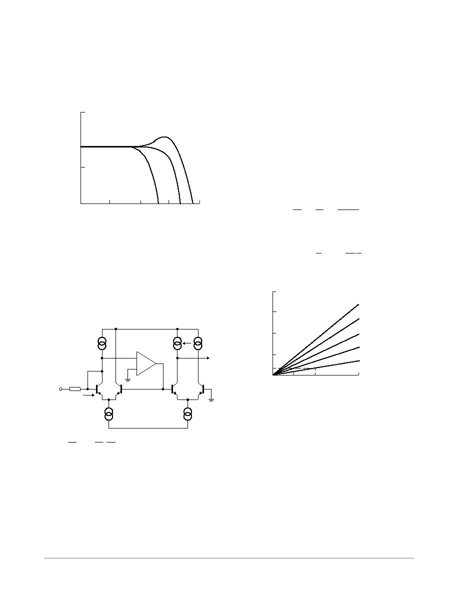
At very high frequencies, the response of the rectifier will
fall off. The rolloff will be more pronounced at lower input
levels due to the increasing amount of gain required to switch
between Q5 or Q6 conducting. The rectifier frequency
response for input levels of 0 dBm, 20 dBm, and 40 dBm
is shown in Figure 11. The response at all three levels is flat
to well above the audio range.
0
3
10 k
1 MEG
INPUT = 0 dBm
20 dBm
40 dBm
FREQUENCY (Hz)
GAIN
ERROR
(dB)
Figure 11. Rectifier Frequency Response
vs. Input Level
VARIABLE GAIN CELL
Figure 12 is a diagram of the variable gain cell. This is a
linearized twoquadrant transconductance multiplier. Q1,
Q2 and the op amp provide a predistorted drive signal for the
gain control pair, Q3 and Q4. The gain is controlled by IG and
a current mirror provides the output current.
V+
V
Q2
Q1
NOTE:
IOUT =
IG
I1
R2
20 k
W
VIN
IIN
I2 ( = 2 I1 )
280
mA
+
I1
140
mA
Q4
Q3
IG
IIN =
VIN
R2
IG
I1
Figure 12. Simplified
DG Cell Schematic
The op amp maintains the base and collector of Q1 at
ground potential (VREF) by controlling the base of Q2. The
input current IIN (= VIN/R2) is thus forced to flow through
Q1 along with the current I1, so IC1 = I1 + IIN. Since I2 has
been set at twice the value of I1, the current through Q2 is:
I2 * (I1 ) IIN) + I1 * IIN + IC2.
The op amp has thus forced a linear current swing between
Q1 and Q2 by providing the proper drive to the base of Q2.
This drive signal will be linear for small signals, but very
nonlinear for large signals, since it is compensating for the
nonlinearity of the differential pair, Q1 and Q2, under large
signal conditions.
The key to the circuit is that this same predistorted drive
signal is applied to the gain control pair, Q3 and Q4. When
two differential pairs of transistors have the same signal
applied, their collector current ratios will be identical
regardless of the magnitude of the currents. This gives us:
I
C1
I
C2
+
I
C4
I
C3
+
I
1 ) IIN
I
1 * IIN
plus the relationships IG = IC3 + IC4 and IOUT = IC4 IC3
will yield the multiplier transfer function,
I
OUT +
I
G
I
1
I
IN +
V
IN
R
2
I
G
I
1
This equation is linear and temperatureinsensitive, but it
assumes ideal transistors.
4
3
2
1
0.34
6
0
+6
4 mV
3 mV
2 mv
1 mV
INPUT LEVEL (dBm)
%
THD
VOS = 5 mV
Figure 13.
DG Cell Distortion vs. Offset Voltage
If the transistors are not perfectly matched, a parabolic,
nonlinearity is generated, which results in second
harmonic distortion. Figure 13 gives an indication of the
magnitude of the distortion caused by a given input level and
offset voltage. The distortion is linearly proportional to the
magnitude of the offset and the input level. Saturation of the
gain cell occurs at a +8.0 dBm level. At a nominal operating
level of 0 dBm, a 1.0 mV offset will yield 0.34% of second
harmonic distortion. Most circuits are somewhat better than
相关PDF资料 |
PDF描述 |
|---|---|
| NE592N14G | IC AMP VIDEO 2STAGE DIFF 14-DIP |
| NL17SH00P5T5G | SINGLE 2-INPUT NAND GATE SOT953 |
| NL17SH04P5T5G | IC GATE INVERTER SGL HS SOT953 |
| NL17SH08P5T5G | SINGLE 2-INPUT NAND GATE SOT953 |
| NL17SH32P5T5G | SINGLE 2-INPUT NAND GATE SOT953 |
相关代理商/技术参数 |
参数描述 |
|---|---|
| NE570DR2G | 功能描述:通信集成电路 - 若干 Dual Gain Compandor Commercial Temp RoHS:否 制造商:Maxim Integrated 类型:Transport Devices 封装 / 箱体:TECSBGA-256 数据速率:100 Mbps 电源电压-最大:1.89 V, 3.465 V 电源电压-最小:1.71 V, 3.135 V 电源电流:50 mA, 225 mA 最大工作温度:+ 85 C 最小工作温度:- 40 C 封装:Tube |
| NE570D-T | 制造商:未知厂家 制造商全称:未知厂家 功能描述:Compander |
| NE570F | 制造商:未知厂家 制造商全称:未知厂家 功能描述:Analog Miscellaneous |
| NE570N | 制造商:NXP Semiconductors 功能描述: |
| NE570N-B | 制造商:未知厂家 制造商全称:未知厂家 功能描述:Compander |
发布紧急采购,3分钟左右您将得到回复。