参数资料
| 型号: | NE57811S/N1,518 |
| 厂商: | NXP Semiconductors |
| 文件页数: | 8/13页 |
| 文件大小: | 0K |
| 描述: | IC DDR TERMINATION SPAK-5 |
| 标准包装: | 2,000 |
| 应用: | 转换器,DDR,DDR2 |
| 输入电压: | 1.6 V ~ 3.6 V |
| 输出数: | 1 |
| 工作温度: | 0°C ~ 70°C |
| 安装类型: | 表面贴装 |
| 封装/外壳: | SPAK-5 |
| 供应商设备封装: | 5-SPAK |
| 包装: | 带卷 (TR) |
| 其它名称: | 935284748518 NE57811S/N1-T NE57811S/N1-T-ND |
�� ��
��
��Philips� Semiconductors�
�Advanced� DDR� memory� termination� power�
�with� shutdown�
�APPLICATION� INFORMATION�
�Product� data�
�NE57811�
�The� NE57811� can� be� used� in� a� variety� of� DDR� memory�
�configurations.� Its� small� footprint,� fast� transient� response� and�
�lessened� need� for� large� bulk� output� capacitance,� makes� it� highly�
�adaptable.� Some� of� these� methods� of� use� are� given� below.�
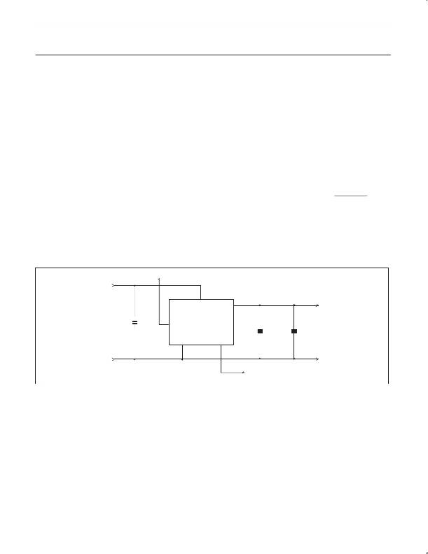
�Normal� operating� mode� (V� TT� =� V� DDR� /2)�
�The� most� common� implementation� of� a� DDR� terminator� regulator�
�using� the� NE57811� is� shown� in� Figure� 10.� The� NE57811� has� an�
�internal� resistor� divider� between� the� V� DD� (pin� 2)� and� V� SS� (pin� 3)� pins�
�which� maintains� the� output� voltage,� V� TT� ,� at� V� DD� /2.� Typically,� the� V� DD�
�voltage� is� the� DDR� RAM� supply� voltage,� which� can� range� from� 1.8� V�
�to� 2.5� V.� The� center� node� of� this� resistor� divider� is� the� reference� for�
�the� V� TT� output� voltage� and� the� buffered� RefOut� signal� (pin� 5).�
�There� are� two� components� to� the� memory� signal� load:� a� high�
�frequency� component� caused� by� the� 266� MHz� plus� speed� of� the�
�address,� data,� and� control� buses,� and� a� low� frequency� component�
�caused� by� the� time-average� skew� of� all� of� the� bus� states� away� from�
�an� equal� number� of� 1s� and� 0s.� Electrolytic� and� tantalum� capacitor�
�appear� inductive� at� the� high� frequencies.� Therefore� two� types� of�
�capacitors� are� needed� for� the� output� filtering.�
�A� very� good,� low� ESR� electrolyic� capacitor� of� no� less� than� 470� μ� F�
�should� be� placed� next� to� the� terminator,� which� should� be� placed� as�
�close� as� possible� to� the� memory� array.� One� half� of� the� high�
�frequency� filter� capacitors� should� be� to� V� DD� and� the� other� half� to�
�SHTDWN�
�V� DD�
�2�
�V� SS� so� that� the� output� will� better� track� any� variations� in� the� V� DD�
�voltage.�
�For� different� memory� sizes,� the� values� of� the� recommended� output�
�filter� capacitances� will� change.� For� a� 256� MByte� memory� space,� for�
�example,� approximately� 100� μ� F� of� ceramic� surface� mount� chip�
�capacitors� should� be� evenly� distributed� across� the� physical� memory�
�layout.� Depending� upon� the� PCB� noise� environment,� this� could� be�
�10� pieces� of� 10� μ� F,� 20� pieces� of� 5� μ� F,� and� so� on.�
�It� might� be� possible� to� reduce� the� total� capacitance,� provided� the�
�performance� remains� stable.� Examine� the� behavior� of� the� V� TT� bus�
�carefully� when� the� system� is� operating� and� verify� that� deviations� in�
�the� bus� voltage� do� not� exceed� the� DDR� specification� (� ±� 40� mV).�
�Use� of� the� SHTDWN� signal� and� low� power� mode�
�The� NE57811� provides� an� optional� SHTDWN� pin� that� may� be� used�
�to� put� the� device� into� low� power� mode.� When� SHUTDOWN� is�
�asserted� (LOW),� the� V� TT� power� amplifier� is� turned� off� and� the� output�
�is� 3-Stated.� This� brings� the� quiescent� current� of� the� entire� device� to�
�less� than� 800� μ� A.�
�If� the� pin� is� not� externally� connected,� and� internal� 10� k� ?� resistor�
�biases� the� control� logic� to� V� DD� causing� the� output� sections� to� be�
�turned� on� and� the� NE57811� operates� normally.�
�(HF)�
�V� DD�
�V� TT�
�1�
�+V� TT�
�NE57811�
�C� IN�
�4�
�SHTDWN�
�C� OUT�
�(LF)�
�C� OUT�
�(HF)�
�GND�
�V� SS�
�3�
�RefOut�
�5�
�GND�
�V� REF�
�SL01694�
�Figure� 10.� Normal� operating� method� (V� TT� =� V� DD� /2)�
�2003� Apr� 02�
�8�
�相关PDF资料 |
PDF描述 |
|---|---|
| ECM36DCTI-S288 | CONN EDGECARD 72POS .156 EXTEND |
| EYM43DTMT | CONN EDGECARD 86POS R/A .156 SLD |
| ECM36DRMT-S664 | CONN EDGECARD 72POS .156 WW |
| GCB60DHNR | CONN EDGECARD 120PS .050 DIP SLD |
| GMM15DRMI-S288 | CONN EDGECARD 30POS .156 EXTEND |
相关代理商/技术参数 |
参数描述 |
|---|---|
| NE57814 | 制造商:PHILIPS 制造商全称:NXP Semiconductors 功能描述:DDR memory termination regulator with standby mode and enhanced efficiency |
| NE57814DD | 制造商:NXP Semiconductors 功能描述: 制造商:NXP Semiconductors 功能描述:DDR TERM W/STANDBY 8SOIC |
| NE57814DD,518 | 功能描述:线性稳压器 - 标准 DDR TERMINATOR REG RoHS:否 制造商:STMicroelectronics 输出类型: 极性: 输出电压:1.8 V 输出电流:150 mA 负载调节: 最大输入电压:5.5 V 线路调整率: 最大工作温度:+ 125 C 安装风格:SMD/SMT 封装 / 箱体:SOT-323-5L |
| NE57814DD518 | 制造商:Rochester Electronics LLC 功能描述: 制造商:NXP 功能描述: 制造商:NXP Semiconductors 功能描述: |
| NE57835 | 制造商:未知厂家 制造商全称:未知厂家 功能描述:TRANSISTOR | BJT | NPN | 11V V(BR)CEO | 30MA I(C) | SOT-173 |
发布紧急采购,3分钟左右您将得到回复。