参数资料
| 型号: | NL17SZ74USG |
| 厂商: | ON Semiconductor |
| 文件页数: | 2/6页 |
| 文件大小: | 0K |
| 描述: | IC FLIP FLOP D-TYPE LOG US8 |
| 标准包装: | 1 |
| 系列: | 17SZ |
| 功能: | 设置(预设)和复位 |
| 类型: | D 型 |
| 输出类型: | 差分 |
| 元件数: | 1 |
| 每个元件的位元数: | 1 |
| 频率 - 时钟: | 250MHz |
| 延迟时间 - 传输: | 2.2ns |
| 触发器类型: | 正边沿 |
| 输出电流高,低: | 32mA,32mA |
| 电源电压: | 1.65 V ~ 5.5 V |
| 工作温度: | -55°C ~ 125°C |
| 安装类型: | 表面贴装 |
| 封装/外壳: | 8-VFSOP(0.091",2.30mm 宽) |
| 包装: | 标准包装 |
| 产品目录页面: | 1126 (CN2011-ZH PDF) |
| 其它名称: | NL17SZ74USGOSDKR |
NL17SZ74
http://onsemi.com
2
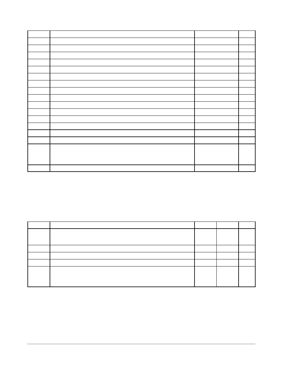
MAXIMUM RATINGS
Symbol
Parameter
Value
Units
VCC
DC Supply Voltage
0.5 to +7.0
V
VI
DC Input Voltage
0.5 to +7.0
V
VO
DC Output Voltage Output in High or Low State (Note 1)
0.5 to VCC +0.5
V
IIK
DC Input Diode Current
VI < GND
50
mA
IOK
DC Output Diode Current
VO < GND
50
mA
IO
DC Output Sink Current
±50
mA
ICC
DC Supply Current Per Supply Pin
±100
mA
IGND
DC Ground Current Per Ground Pin
±100
mA
TSTG
Storage Temperature Range
65 to +150
°C
TL
Lead Temperature, 1 mm from Case for 10 Seconds
260
°C
TJ
Junction Temperature Under Bias
+150
°C
qJA
Thermal Resistance (Note 2)
250
°C/W
PD
Power Dissipation in Still Air at 85°C
250
mW
MSL
Moisture Sensitivity
Level 1
FR
Flammability Rating, Oxygen Index: 28 to 34
UL 94 V0 @ 0.125 in
VESD
ESD Withstand Voltage
Human Body Model (Note 3)
Machine Model (Note 4)
Charged Device Model (Note 5)
>4000
>200
N/A
V
ILATCHUP
±100
mA
Stresses exceeding Maximum Ratings may damage the device. Maximum Ratings are stress ratings only. Functional operation above the
Recommended Operating Conditions is not implied. Extended exposure to stresses above the Recommended Operating Conditions may affect
device reliability.
1. IO absolute maximum rating must be observed.
2. Measured with minimum pad spacing on an FR4 board, using 10 mm X 1 inch, 2 ounce copper trace with no air flow.
3. Tested to EIA/JESD22A114A.
4. Tested to EIA/JESD22A115A.
5. Tested to JESD22C101A.
6. Tested to EIA/JESD78.
RECOMMENDED OPERATING CONDITIONS
Symbol
Parameter
Min
Max
Units
VCC
Supply Voltage
Operating
Data Retention Only
1.65
1.5
5.5
V
VI
Input Voltage (Note 7)
0
5.5
V
VO
Output Voltage (HIGH or LOW State)
0
5.5
V
TA
Operating FreeAir Temperature
55
+125
°C
Dt/DV
Input Transition Rise or Fall Rate
VCC = 2.5 V ±0.2 V
VCC = 3.0 V ±0.3 V
VCC = 5.0 V ±0.5 V
0
20
10
5.0
ns/V
7. Unused inputs may not be left open. All inputs must be tied to a highlogic voltage level or a lowlogic input voltage level.
相关PDF资料 |
PDF描述 |
|---|---|
| NC7SZ175L6X | IC FLIP FLOP UHS D 6-MICROPAK |
| 535P | TERMINATOR MALE 8A 600V |
| M85049/31-18N | E NUT SHELL SIZE 18 NICKEL |
| V48A3V3M264BG | CONVERTER MOD DC/DC 3.3V 264W |
| V48A3V3M264BF3 | CONVERTER MOD DC/DC 3.3V 264W |
相关代理商/技术参数 |
参数描述 |
|---|---|
| NL17SZ74USG | 制造商:ON Semiconductor 功能描述:Analog Switch IC |
| NL17SZ74USG-CUT TAPE | 制造商:ON 功能描述:NL17SZ Series 3.25 V Surface Mount Single D-Type Flip-Flop - US-8 |
| NL17SZ74USGH | 制造商:Rochester Electronics LLC 功能描述: 制造商:ON Semiconductor 功能描述: |
| NL17SZ86 | 制造商:ONSEMI 制造商全称:ON Semiconductor 功能描述:Single 2-Input Exclusive-OR Gate |
| NL17SZ86/D | 制造商:未知厂家 制造商全称:未知厂家 功能描述:Single 2-Input Exclusive-OR Gate |
发布紧急采购,3分钟左右您将得到回复。