- 您现在的位置:买卖IC网 > PDF目录18987 > NOII5FM1300A-QDC (ON Semiconductor)SENSOR IMAGE 1.3MP CMOS 84-LCC PDF资料下载
参数资料
| 型号: | NOII5FM1300A-QDC |
| 厂商: | ON Semiconductor |
| 文件页数: | 19/33页 |
| 文件大小: | 0K |
| 描述: | SENSOR IMAGE 1.3MP CMOS 84-LCC |
| 标准包装: | 1 |
| 象素大小: | 6.7µm x 6.7µm |
| 有源象素阵列: | 1280H x 1024V |
| 每秒帧数: | 27 |
| 电源电压: | 3 V ~ 4.5 V |
| 类型: | CMOS 成像 |
| 封装/外壳: | 84-LCC |
| 供应商设备封装: | 84-LCC(18x18) |
| 包装: | 托盘 |
| 请注意: | * |
| 其它名称: | CYII5FM1300AB-QDC CYII5FM1300AB-QDC-ND |
第1页第2页第3页第4页第5页第6页第7页第8页第9页第10页第11页第12页第13页第14页第15页第16页第17页第18页当前第19页第20页第21页第22页第23页第24页第25页第26页第27页第28页第29页第30页第31页第32页第33页
�� �
�
�NOII5SM1300A�
�Sync� of� left� shift-register�
�Sync� of� right� shift-register�
�Last� line,� followed� by�
�sync� of� left� shift-register�
�Line� n�
�T� reg_int�
�Sync�
�T� int�
�Figure� 18.� Synchronization� of� Shift� Registers� in� Rolling� Shutter� Mode�
�X_REG� Register� (10:0)�
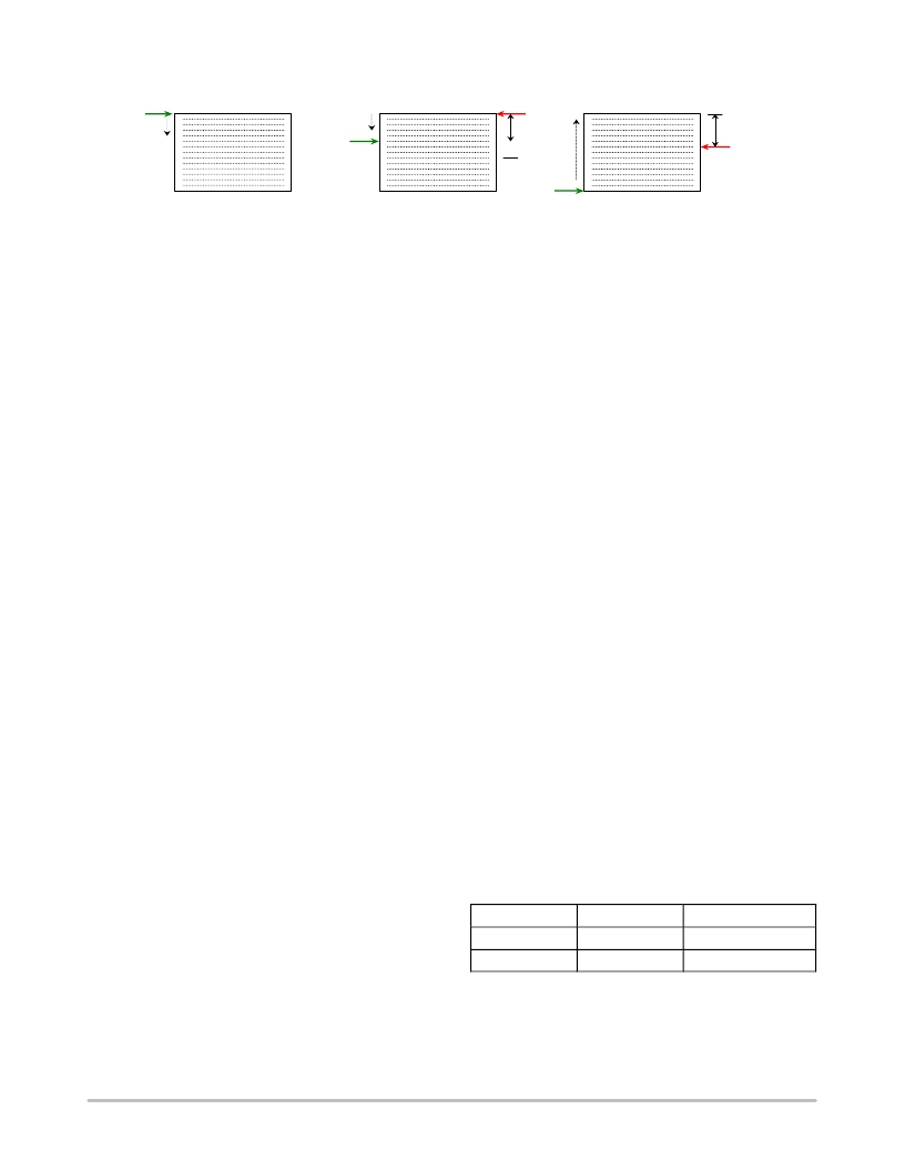
�The� X_REG� register� determines� the� start� position� of� the�
�window� in� the� X-direction.� In� this� direction,� there� are� 640�
�possible� starting� positions� (two� pixels� are� addressed� at� the�
�same� time� in� one� clock� cycle).� If� sub� sampling� is� enabled,�
�only� the� even� pixels� are� set� as� starting� position� (for� instance:�
�0,� 2,� 4,� 6,� 8� …� 638).�
�YL_REG� (10:0)� and� YR_REG� (10:0)�
�The� YL_REG� and� YR_REG� registers� determine� the� start�
�position� of� the� window� in� the� Y-direction.� In� this� direction,�
�there� are� 1024� possible� starting� positions.� In� rolling� shutter�
�mode� the� YL_REG� register� sets� the� start� position� of� the� read�
�(left)� pointer� and� the� YR_REG� sets� the� start� position� of� the�
�reset� (right)� pointer.� For� both� shutter� types� YL_REG� is�
�always� equal� to� YR_REG.�
�Image� Core� Register� (7:0)�
�Bits� 1:0� of� the� IMAGE_CORE� register� define� the� test�
�mode� of� the� image� core.� Setting� 00� is� the� default� and� normal�
�operation� mode.� In� case� the� bit� is� set� to� ‘1’,� the� odd� (bit� 1)�
�or� even� (bit� 0)� columns� are� tight� to� the� reset� level.� If� the�
�internal� ADC� is� used,� bits� 0� and� 1� are� used� to� create� test�
�pattern� to� test� the� sample� moment� of� the� ADC.� If� the� ADC�
�sample� moment� is� not� chosen� correctly,� the� created� test�
�pattern� is� not� black-white-black-etc.� (IMAGE_CORE�
�register� set� at� 1� or� 2)� or�
�black-black-white-white-black-black� (IMAGE_CORE�
�register� set� at� 9)� but� grey� shadings� if� the� sensor� is� saturated.�
�Bits� 7:2� of� the� IMAGE_CORE� register� define� the�
�sub-sampling� mode� in� the� X-direction� (bits� 4:2)� and� in� the�
�Y-direction� (bits� 7:5).� The� sub-sampling� modes� and�
�corresponding� bit� setting� are� given� in� Table� 11� and� Table� 12�
�on� page� 11.�
�Amplifier� Register� (6:0)�
�1.� GAIN� (bits� 3:0)�
�The� gain� bits� determine� the� gain� setting� of� the� output�
�amplifier.� They� are� only� effective� if� UNITY� =� 0.� The�
�gains� and� corresponding� bit� setting� are� given� in�
�Table� 13� on� page� 12.�
�connects� to� ADC_IN.� The� gain� amplifier� and� output�
�driver� of� the� second� path� are� put� in� standby.�
�4.� STANDBY�
�If� STANDBY� =� 0,� the� complete� output� amplifier� is�
�put� in� standby.� For� normal� use,� set� STANDBY� to� ‘1’.�
�DAC_RAW� Register� (6:0)� and� DAC_FINE� (6:0)�
�Register�
�These� registers� determine� the� black� reference� level� at� the�
�output� of� the� output� amplifier.� Bit� setting� 1111111� for� the�
�DAC_RAW� register� gives� the� highest� offset� voltage.� Bit�
�setting� 0000000� for� the� DAC_RAW� register� gives� the� lowest�
�offset� voltage.� Ideally,� if� the� two� output� paths� have� no� offset�
�mismatch,� the� DAC_FINE� register� is� set� to� 1000000.�
�Deviation� from� this� value� is� used� to� compensate� the� internal�
�mismatch� (see� Output� Amplifier� on� page� 12).�
�ADC� Register� (2:0)�
�1.� TRISTATE_OUT� (bit� 0)�
�In� case� TRISTATE� =� 0,� the� ADC_D<9:0>� outputs� are�
�in� tri-state� mode.� TRISTATE� =� 1� for� normal� operation�
�mode.�
�2.� GAMMA� (bit� 1)�
�If� GAMMA� is� set� to� ‘1’,� the� ADC� input� to� output�
�conversion� is� linear;� otherwise� the� conversion� follows�
�a� ‘gamma’� law� (more� contrast� in� dark� parts� of� the�
�window,� lower� contrast� in� the� bright� parts).�
�3.� BIT_INV� (bit� 2)�
�If� BIT_INV� =� 1,� 0000000000� is� the� conversion� of� the�
�lowest� possible� input� voltage,� otherwise� the� bits� are�
�inverted.�
�Data� Interfaces�
�Two� different� data� interfaces� are� implemented.� They� are�
�selected� using� pins� IF_MODE� (pin� 12)� and� SER_MODE�
�(pin� 6).�
�Table� 19.� SERIAL� AND� PARALLEL� INTERFACE�
�SELECTION�
�IF_MODE� SER_MODE� Selected� interface�
�2.� UNITY� (bit� 4)�
�In� case� UNITY� =� 1,� the� gain� setting� of� GAIN� is�
�bypassed� and� the� gain� amplifier� is� put� in� unity� feedback.�
�1�
�0�
�X�
�1�
�Parallel�
�Serial� 3� Wire�
�3.� DUAL_OUT� (bit� 5)�
�If� DUAL_OUT� =� 1,� the� two� output� amplifiers� are�
�active.� If� DUAL_OUT� =� 0,� the� signals� from� the� two�
�buses� are� multiplexed� to� output� PXL_OUT1� which�
�Parallel� Interface�
�The� parallel� interface� uses� a� 16-bit� parallel� input�
�(P_DATA� (15:0))� to� upload� new� register� values.� Asserting�
�http://onsemi.com�
�19�
�相关PDF资料 |
PDF描述 |
|---|---|
| CT4-MLXM | LINKING CABLE 4WAY-8WAY MALE |
| MT9T031P12STC | IC SENSOR IMAGE COLOR 48-PLCC |
| MT9V022I77ATM | IC SENSOR IMAGE VGA MONO 52IBGA |
| MT9V022I77ATC | IC SENSOR IMAGE VGA COLOR 52IBGA |
| ASFL1-66.666MHZ-L-T | OSCILLATOR 66.666 MHZ 3.3V SMD |
相关代理商/技术参数 |
参数描述 |
|---|---|
| NOII5SC1300A-QDC | 功能描述:SENSOR IMAGE COLOR CMOS 84-LCC RoHS:否 类别:传感器,转换器 >> 图像,相机 系列:- 标准包装:480 系列:- 象素大小:6.7µm x 6.7µm 有源象素阵列:768H x 488V 每秒帧数:52 电源电压:3.3V 类型:CMOS 成像 封装/外壳:48-QFP 供应商设备封装:48-QFP 包装:托盘 请注意:* 配用:4H2105-ND - HEADBOARD FOR KAC-004014H2104-ND - KIT EVAL FOR KAC-00401 其它名称:4H20954H2095-NDKAC-00401-CBC-LB-A0 |
| NOII5SM1300A-QDC | 功能描述:SENSOR IMAGE MONO CMOS 84-LCC RoHS:否 类别:传感器,转换器 >> 图像,相机 系列:- 标准包装:480 系列:- 象素大小:6.7µm x 6.7µm 有源象素阵列:768H x 488V 每秒帧数:52 电源电压:3.3V 类型:CMOS 成像 封装/外壳:48-QFP 供应商设备封装:48-QFP 包装:托盘 请注意:* 配用:4H2105-ND - HEADBOARD FOR KAC-004014H2104-ND - KIT EVAL FOR KAC-00401 其它名称:4H20954H2095-NDKAC-00401-CBC-LB-A0 |
| NOIL1SC4000A-GDC | 功能描述:IC IMAGE SENSOR 4MP 127-PGA RoHS:是 类别:传感器,转换器 >> 图像,相机 系列:* 标准包装:480 系列:- 象素大小:6.7µm x 6.7µm 有源象素阵列:768H x 488V 每秒帧数:52 电源电压:3.3V 类型:CMOS 成像 封装/外壳:48-QFP 供应商设备封装:48-QFP 包装:托盘 请注意:* 配用:4H2105-ND - HEADBOARD FOR KAC-004014H2104-ND - KIT EVAL FOR KAC-00401 其它名称:4H20954H2095-NDKAC-00401-CBC-LB-A0 |
| NOIL1SE0300A-QDC | 功能描述:SENSOR IMAGE COLOR CMOS 48-LCC RoHS:否 类别:传感器,转换器 >> 图像,相机 系列:- 标准包装:480 系列:- 象素大小:6.7µm x 6.7µm 有源象素阵列:768H x 488V 每秒帧数:52 电源电压:3.3V 类型:CMOS 成像 封装/外壳:48-QFP 供应商设备封装:48-QFP 包装:托盘 请注意:* 配用:4H2105-ND - HEADBOARD FOR KAC-004014H2104-ND - KIT EVAL FOR KAC-00401 其它名称:4H20954H2095-NDKAC-00401-CBC-LB-A0 |
| NOIL1SE3000A-GDC | 功能描述:IC IMAGE SENSOR 3MP 369-PGA RoHS:是 类别:传感器,转换器 >> 图像,相机 系列:* 标准包装:480 系列:- 象素大小:6.7µm x 6.7µm 有源象素阵列:768H x 488V 每秒帧数:52 电源电压:3.3V 类型:CMOS 成像 封装/外壳:48-QFP 供应商设备封装:48-QFP 包装:托盘 请注意:* 配用:4H2105-ND - HEADBOARD FOR KAC-004014H2104-ND - KIT EVAL FOR KAC-00401 其它名称:4H20954H2095-NDKAC-00401-CBC-LB-A0 |
发布紧急采购,3分钟左右您将得到回复。