- 您现在的位置:买卖IC网 > Datasheet目录484 > NOIL1SC4000A-GDC (ON Semiconductor)IC IMAGE SENSOR 4MP 127-PGA Datasheet资料下载
参数资料
| 型号: | NOIL1SC4000A-GDC |
| 厂商: | ON Semiconductor |
| 文件页数: | 10/30页 |
| 文件大小: | 0K |
| 描述: | IC IMAGE SENSOR 4MP 127-PGA |
| 标准包装: | 1 |
| 系列: | * |
| 象素大小: | 12µm x 12µm |
| 有源象素阵列: | 2048H x 2048V |
| 每秒帧数: | 15 |
| 电源电压: | 2.5V, 3.3V |
| 类型: | CMOS 成像 |
| 封装/外壳: | * |
| 供应商设备封装: | * |
| 包装: | * |
| 其它名称: | CYIL1SC4000AA-GDC CYIL1SC4000AA-GDC-ND |
第1页第2页第3页第4页第5页第6页第7页第8页第9页当前第10页第11页第12页第13页第14页第15页第16页第17页第18页第19页第20页第21页第22页第23页第24页第25页第26页第27页第28页第29页第30页
�� �
�
�NOIL1SM4000A�
�Biasing� and� Analog� Signals�
�The� expected� analog� output� levels� are� between� 0.3� V� for�
�a� white,� saturated,� pixel� and� 1.3� V� for� a� black� pixel.�
�There� are� two� output� stages,� each� consisting� of� two� output�
�amplifiers,� resulting� in� four� outputs.� One� output� amplifier� is�
�used� for� the� analog� signal� resulting� from� the� pixels.� The�
�second� amplifier� is� used� for� a� DC� reference� signal.� The� DC�
�level� from� the� buffer� is� defined� by� a� DAC,� which� is�
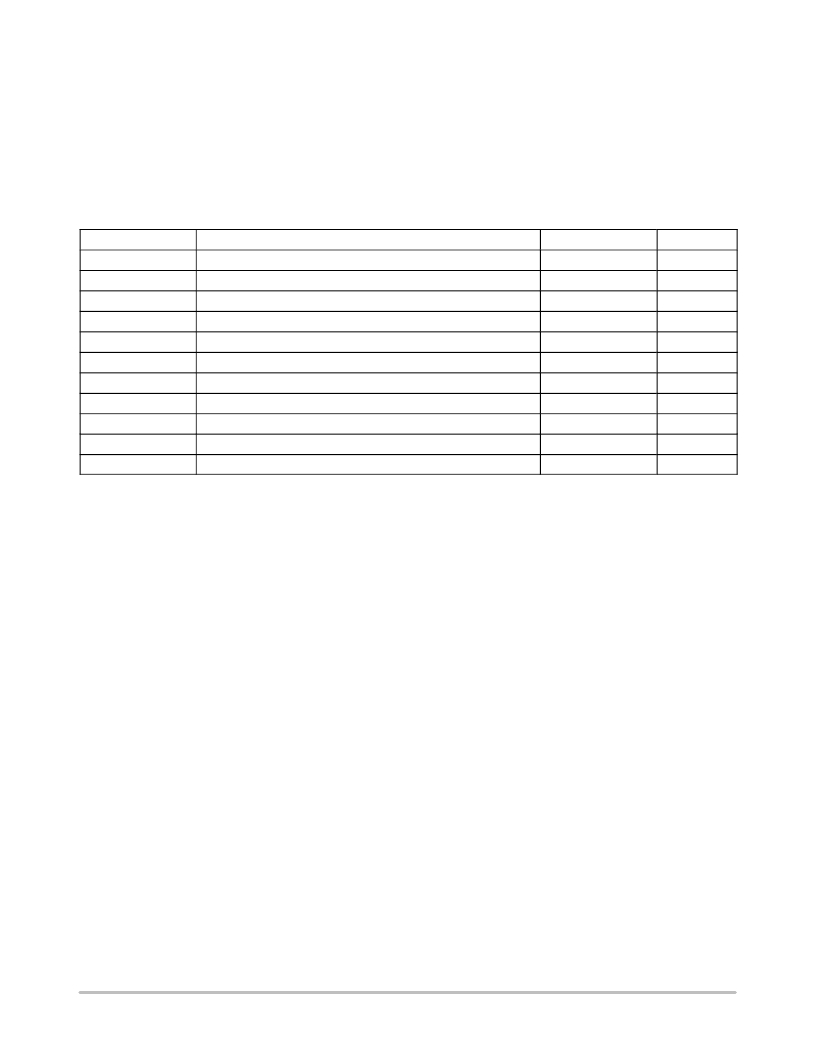
�Table 3. OVERVIEW� OF� BIAS� SIGNALS�
�controlled� by� a� 7-bit� word� downloaded� in� the� SPI.�
�Additionally,� an� extra� bit� in� the� SPI� defines� if� one� or� two�
�output� stages� are� used.�
�Table� 3� summarizes� the� biasing� signals� required� to� drive�
�this� image� sensor.� To� optimize� biasing� of� column� amplifiers�
�to� power� dissipation,� several� biasing� resistors� are� required.�
�This� optimisation� results� in� an� increase� of� signal� swing� and�
�dynamic� range.�
�Signal�
�Out_load�
�dec_x_load�
�muxbus_load�
�nsf_load�
�uni_load_fast�
�uni_load�
�pre_load�
�col_load�
�dec_y_load�
�psf_load�
�precharge_bias�
�Comment�
�Connect� with� 60� K� W� to� Voo� and� capacitor� of� 100� nF� to� Gnd�
�Connect� with� 2� M� W� to� Vdd� and� capacitor� of� 100� nF� to� Gnd�
�Connect� with� 25� K� W� to� Vaa� and� capacitor� of� 100� nF� to� Gnd�
�Connect� with� 5� K� W� to� Vaa� and� capacitor� of� 100� nF� to� Gnd�
�Connect� with� 10� K� W� to� Vaa� and� capacitor� of� 100� nF� to� Gnd�
�Connect� with� 1� M� W� to� Vaa� and� capacitor� of� 100� nF� to� Gnd�
�Connect� with� 3� K� W� to� Vaa� and� capacitor� of� 100� nF� to� Gnd�
�Connect� with� 1� M� W� to� Vaa� and� capacitor� of� 100� nF� to� Gnd�
�Connect� with� 2� M� W� to� Vdd� and� capacitor� of� 100� nF� to� Gnd�
�Connect� with� 1� M� W� to� Vaa� and� capacitor� of� 100� nF� to� Gnd�
�Connect� with� 1� k� W� to� Vdd� and� capacitor� of� at� least� 200� nF� to� Gnd�
�Related� Module�
�Output� stage�
�X-addressing�
�Multiplex� bus�
�Column� amplifiers�
�Column� amplifiers�
�Column� amplifiers�
�Column� amplifiers�
�Column� amplifiers�
�Y-addressing�
�Column� amplifiers�
�Pixel� drivers�
�DC� Level�
�0.7� V�
�0.4� V�
�0.8� V�
�1.2� V�
�1.2� V�
�0.5� V�
�1.4� V�
�0.5� V�
�0.4� V�
�0.5� V�
�1.4� V�
�Each� biasing� signal� determines� the� operation� of� a�
�corresponding� module� in� the� sense� that� it� controls� speed� and�
�dissipation.� Some� modules� have� two� biasing� resistors:� one�
�to� achieve� the� high� speed� and� another� to� minimize� power�
�dissipation.�
�Pixel� Array� Signals�
�The� pixel� array� of� the� image� sensor� requires� digital� control�
�signals� and� several� different� power� supplies.� This� section�
�explains� the� relation� between� the� control� signals� and� the�
�applied� supplies,� and� the� internal� generated� pixel� array�
�signals.�
�Figure� 11� illustrates� the� internal� generated� pixel� array�
�signals:� Reset,� Sample,� Precharge,� Vmem,� and� Row_select.�
�These� are� internal� generated� signals� derived� by� on-chip�
�drivers� from� external� applied� signals.� Row_select� is�
�generated� by� the� y-addressing� and� is� not� discussed� in� this�
�section�
�Reset:� Resets� the� pixel� and� initiates� the� integration� time.�
�If� reset� is� high,� then� the� photodiode� is� forced� to� a� certain�
�voltage.� This� depends� on� Vpix� (pixel� supply)� and� the� high�
�level� of� reset� signal.� The� higher� these� signals� or� supplies,�
�the� higher� the� voltage-swing.� The� limitation� on� the� high�
�level� of� reset� and� Vpix� is� 3.3� V.� It� does� not� help� to� increase�
�Vpix� without� increasing� the� reset� level.� The� opposite� is� true.�
�Additionally,� it� is� the� reset� pulse� that� also� controls� the� dual�
�or� multiple� slope� feature� inside� the� pixel.� By� giving� a� reset�
�pulse� during� integration,� but� not� at� full� reset� level,� the�
�photodiode� is� reset� to� a� new� value,� only� if� this� value� is�
�decreased� due� to� light� illumination.�
�The� low� level� of� reset� is� 0� V,� but� the� high� level� is� 2.5� V� or�
�higher� (3.3� V)� for� the� normal� reset� and� a� lower� (<2.5� V)� level�
�for� the� multiple� slope� reset.�
�Precharge:� Precharge� serves� as� a� load� for� the� first� source�
�follower� in� the� pixel� and� is� activated� to� overwrite� the� current�
�information� on� the� storage� node� by� the� new� information� on�
�the� photodiode.� Precharge� is� controlled� by� an� external�
�digital� signal� between� 0� V� and� 2.5� V.�
�Sample:� Samples� the� photodiode� information� onto� the�
�memory� element.� This� signal� is� also� a� standard� digital� level�
�between� 0� V� and� 2.5� V.�
�Vmem:� This� signal� increases� the� information� on� the�
�memory� element� with� a� certain� offset.� This� increases� the�
�output� voltage� variation.� Vmem� changes� between� Vmem_l�
�(2.5� V)� and� Vmem_h� (3.3� V).�
�http://onsemi.com�
�10�
�相关PDF资料 |
PDF描述 |
|---|---|
| NOIL1SE3000A-GDC | IC IMAGE SENSOR 3MP 369-PGA |
| NOIL1SM0300A-WWC | IC IMAGE SENSOR LUPA300 48LLC |
| NOIL2SC1300A-GDC | IC IMAGE SENSOR LUPA1300 168PGA |
| NOIV1SE025KA-GDC | IC IMAGE SENSOR 25MP 355PGA |
| NP100P04PDG-E1-AY | MOSFET P-CH -40V MP-25ZP/TO-263 |
相关代理商/技术参数 |
参数描述 |
|---|---|
| NOIL1SE0300A-QDC | 功能描述:SENSOR IMAGE COLOR CMOS 48-LCC RoHS:否 类别:传感器,转换器 >> 图像,相机 系列:- 标准包装:480 系列:- 象素大小:6.7µm x 6.7µm 有源象素阵列:768H x 488V 每秒帧数:52 电源电压:3.3V 类型:CMOS 成像 封装/外壳:48-QFP 供应商设备封装:48-QFP 包装:托盘 请注意:* 配用:4H2105-ND - HEADBOARD FOR KAC-004014H2104-ND - KIT EVAL FOR KAC-00401 其它名称:4H20954H2095-NDKAC-00401-CBC-LB-A0 |
| NOIL1SE3000A-GDC | 功能描述:IC IMAGE SENSOR 3MP 369-PGA RoHS:是 类别:传感器,转换器 >> 图像,相机 系列:* 标准包装:480 系列:- 象素大小:6.7µm x 6.7µm 有源象素阵列:768H x 488V 每秒帧数:52 电源电压:3.3V 类型:CMOS 成像 封装/外壳:48-QFP 供应商设备封装:48-QFP 包装:托盘 请注意:* 配用:4H2105-ND - HEADBOARD FOR KAC-004014H2104-ND - KIT EVAL FOR KAC-00401 其它名称:4H20954H2095-NDKAC-00401-CBC-LB-A0 |
| NOIL1SM0300A-QDC | 功能描述:IC IMAGE SENSOR LUPA300 48LLC RoHS:是 类别:传感器,转换器 >> 图像,相机 系列:* 标准包装:480 系列:- 象素大小:6.7µm x 6.7µm 有源象素阵列:768H x 488V 每秒帧数:52 电源电压:3.3V 类型:CMOS 成像 封装/外壳:48-QFP 供应商设备封装:48-QFP 包装:托盘 请注意:* 配用:4H2105-ND - HEADBOARD FOR KAC-004014H2104-ND - KIT EVAL FOR KAC-00401 其它名称:4H20954H2095-NDKAC-00401-CBC-LB-A0 |
| NOIL1SM0300A-WWC | 功能描述:IC IMAGE SENSOR LUPA300 48LLC RoHS:是 类别:传感器,转换器 >> 图像,相机 系列:LUPA300 标准包装:480 系列:- 象素大小:6.7µm x 6.7µm 有源象素阵列:768H x 488V 每秒帧数:52 电源电压:3.3V 类型:CMOS 成像 封装/外壳:48-QFP 供应商设备封装:48-QFP 包装:托盘 请注意:* 配用:4H2105-ND - HEADBOARD FOR KAC-004014H2104-ND - KIT EVAL FOR KAC-00401 其它名称:4H20954H2095-NDKAC-00401-CBC-LB-A0 |
| NOIL1SM1300AWES | 制造商:ON Semiconductor 功能描述:PW/H |
发布紧急采购,3分钟左右您将得到回复。