- 您现在的位置:买卖IC网 > PDF目录363669 > NT5SV16M16AT-8BL (Electronic Theatre Controls, Inc.) 256Mb Synchronous DRAM PDF资料下载
参数资料
| 型号: | NT5SV16M16AT-8BL |
| 厂商: | Electronic Theatre Controls, Inc. |
| 英文描述: | 256Mb Synchronous DRAM |
| 中文描述: | 256Mb的同步DRAM |
| 文件页数: | 9/65页 |
| 文件大小: | 814K |
| 代理商: | NT5SV16M16AT-8BL |
第1页第2页第3页第4页第5页第6页第7页第8页当前第9页第10页第11页第12页第13页第14页第15页第16页第17页第18页第19页第20页第21页第22页第23页第24页第25页第26页第27页第28页第29页第30页第31页第32页第33页第34页第35页第36页第37页第38页第39页第40页第41页第42页第43页第44页第45页第46页第47页第48页第49页第50页第51页第52页第53页第54页第55页第56页第57页第58页第59页第60页第61页第62页第63页第64页第65页
NT5SV64M4AT(L)
NT5SV32M8AT(L)
NT5SV16M16AT(L)
256Mb Synchronous DRAM
REV 1.0
May, 2001
9
NANYA TECHNOLOGY CORP
. All rights reserved.
NANYA TECHNOLOGY CORP. reserves the right to change Products and Specifications without notice.
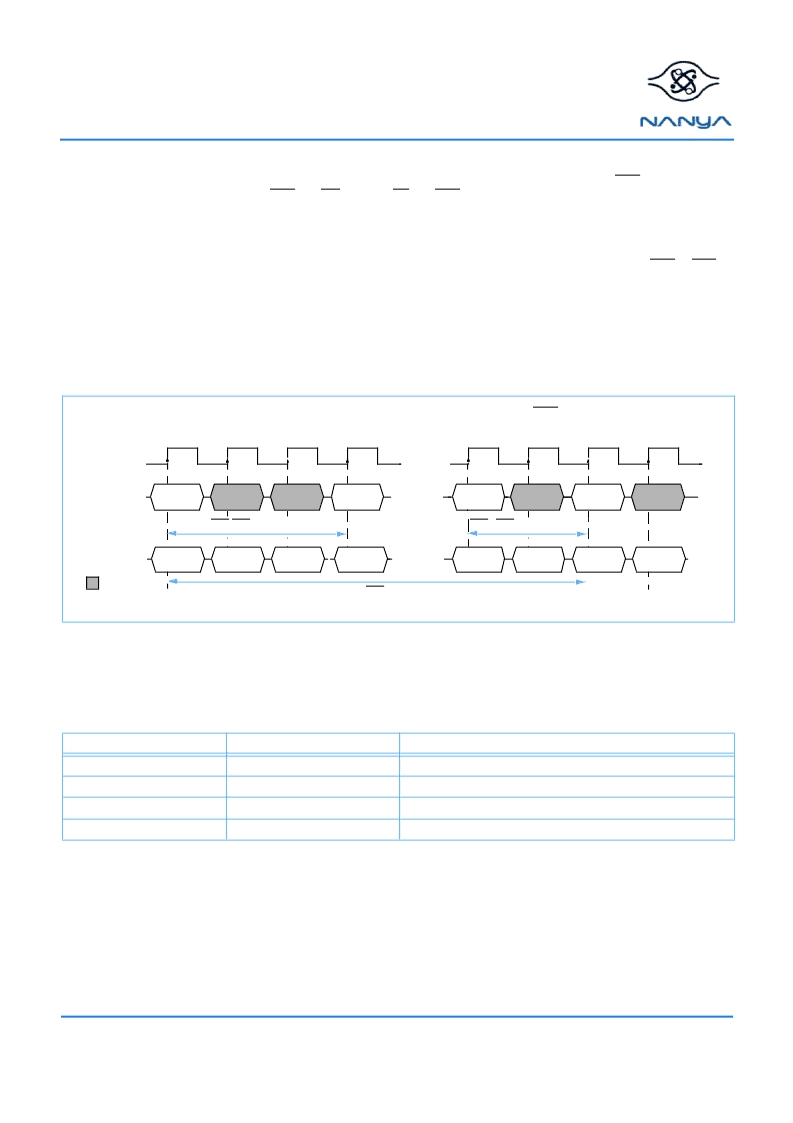
Bank Activate Command
In relation to the operation of a fast page mode DRAM, the Bank Activate command correlates to a falling RAS signal.
The Bank
Activate command is issued by holding CAS and WE high with CS and RAS low at the rising edge of the clock. The Bank Select
address BA0 - BA1 is used to select the desired bank. The row address A0 - A12 is used to determine which row to activate in
the selected bank.
The Bank Activate command must be applied before any Read or Write operation can be executed. The delay from when the
Bank Activate command is applied to when the first read or write operation can begin must meet or exceed the RAS to CAS
delay time (t
RCD
). Once a bank has been activated it must be precharged before another Bank Activate command can be
applied to the same bank. The minimum time interval between successive Bank Activate commands to the same bank is deter-
mined by the RAS cycle time of the device (t
RC
). The minimum time interval between interleaved Bank Activate commands
(Bank A to Bank B and vice versa) is the Bank to Bank delay time (t
RRD
). The maximum time that each bank can be held active
is specified as t
RAS(max)
.
Bank Select
The Bank Select inputs, BA0 and BA1, determine the bank to be used during a Bank Activate, Precharge, Read, or Write oper-
ation.
Bank Activate Command Cycle
Bank Selection Bits
BA0
BA1
Bank
0
0
Bank 0
1
0
Bank 1
0
1
Bank 2
1
1
Bank 3
ADDRESS
CK
T0
T2
T1
T3
Tn
Tn+1
Tn+2
Tn+3
COMMAND
NOP
NOP
NOP
NOP
Bank A
Row Addr.
Bank A
Activate
PWrite A
Bank A
Col. Addr.
. . . . . . . . . .
. . . . . . . . . .
. . . . . . . . . .
Bank B
Activate
Bank A
Row Addr.
Bank A
Activate
RAS-CAS delay (
t
RCD
)
: “H” or “L”
RAS Cycle time (
t
RC
)
RAS - RAS delay time (
t
RRD
)
Bank B
Row Addr.
(CAS Latency = 3, t
RCD
= 3)
相关PDF资料 |
PDF描述 |
|---|---|
| NT5SV32M8AT | 256Mb Synchronous DRAM |
| NT5SV32M8AT-75B | 256Mb Synchronous DRAM |
| NT5SV32M8AT-7K | 256Mb Synchronous DRAM |
| NT5SV32M8AT-8B | 256Mb Synchronous DRAM |
| NT5SV64M4AT | 256Mb Synchronous DRAM |
相关代理商/技术参数 |
参数描述 |
|---|---|
| NT5SV16M4DT | 制造商:未知厂家 制造商全称:未知厂家 功能描述:64Mb Synchronous DRAM |
| NT5SV16M4DT-6K | 制造商:未知厂家 制造商全称:未知厂家 功能描述:64Mb Synchronous DRAM |
| NT5SV16M4DT-7 | 制造商:未知厂家 制造商全称:未知厂家 功能描述:64Mb Synchronous DRAM |
| NT5SV16M4DT-7K | 制造商:未知厂家 制造商全称:未知厂家 功能描述:64Mb Synchronous DRAM |
| NT5SV32M8AT | 制造商:未知厂家 制造商全称:未知厂家 功能描述:256Mb Synchronous DRAM |
发布紧急采购,3分钟左右您将得到回复。