- 您现在的位置:买卖IC网 > PDF目录17490 > NTB75N06LT4 (ON Semiconductor)MOSFET N-CH 60V 75A D2PAK PDF资料下载
参数资料
| 型号: | NTB75N06LT4 |
| 厂商: | ON Semiconductor |
| 文件页数: | 1/7页 |
| 文件大小: | 0K |
| 描述: | MOSFET N-CH 60V 75A D2PAK |
| 产品变化通告: | Product Obsolescence 30/Dec/2003 Discontinuation 30/Jun/2006 |
| 标准包装: | 800 |
| FET 型: | MOSFET N 通道,金属氧化物 |
| FET 特点: | 逻辑电平门 |
| 漏极至源极电压(Vdss): | 60V |
| 电流 - 连续漏极(Id) @ 25° C: | 75A |
| 开态Rds(最大)@ Id, Vgs @ 25° C: | 11 毫欧 @ 37.5A,5V |
| Id 时的 Vgs(th)(最大): | 2V @ 250µA |
| 闸电荷(Qg) @ Vgs: | 92nC @ 5V |
| 输入电容 (Ciss) @ Vds: | 4370pF @ 25V |
| 功率 - 最大: | 2.4W |
| 安装类型: | 表面贴装 |
| 封装/外壳: | TO-263-3,D²Pak(2 引线+接片),TO-263AB |
| 供应商设备封装: | D2PAK |
| 包装: | 带卷 (TR) |
| 其它名称: | NTB75N06LT4OS |
�� �
�
�NTP75N06L,� NTB75N06L�
�Power� MOSFET�
�75� Amps,� 60� Volts,� Logic�
�Level�
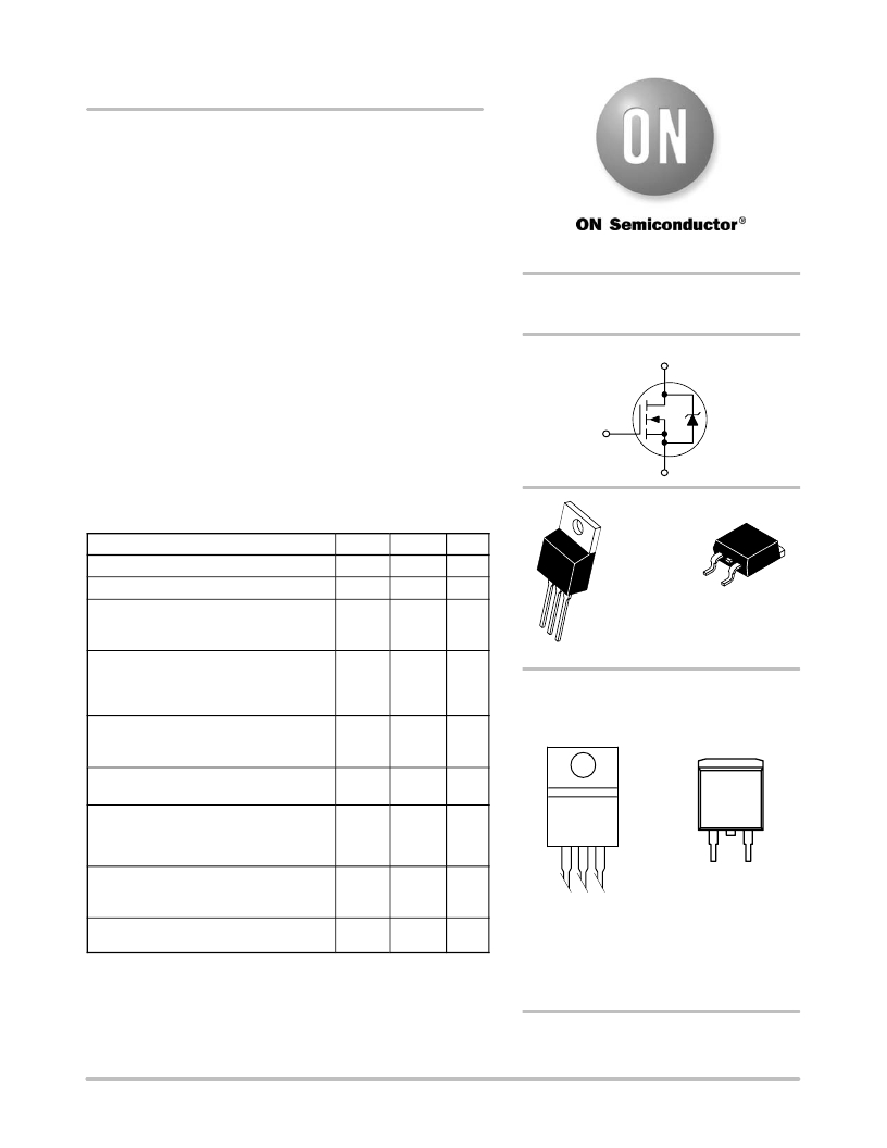
�N?Channel� TO?220� and� D� 2� PAK�
�Designed� for� low� voltage,� high� speed� switching� applications� in�
�power� supplies,� converters� and� power� motor� controls� and� bridge�
�circuits.�
�Features�
�?� Pb?Free� Packages� are� Available�
�Typical� Applications�
�http://onsemi.com�
�75� AMPERES,� 60� VOLTS�
�R� DS(on)� =� 11� m� W�
�N?Channel�
�D�
�?�
�?�
�?�
�?�
�Power� Supplies�
�Converters�
�Power� Motor� Controls�
�Bridge� Circuits�
�G�
�S�
�4�
�MAXIMUM� RATINGS� (T� J� =� 25� °� C� unless� otherwise� noted)�
�Rating�
�Symbol�
�Value�
�Unit�
�4�
�Drain?to?Source� Voltage�
�Drain?to?Gate� Voltage� (R� GS� =� 10� M� W� )�
�V� DSS�
�V� DGR�
�60�
�60�
�Vdc�
�Vdc�
�1�
�2�
�3�
�Gate?to?Source� Voltage�
�?� Continuous�
�?� Non?Repetitive� (t� p� v� 10� ms)�
�Drain� Current�
�?� Continuous� @� T� A� =� 25� °� C�
�?� Continuous� @� T� A� =� 100� °� C�
�?� Single� Pulse� (t� p� v� 10� m� s)�
�Total� Power� Dissipation� @� T� A� =� 25� °� C�
�Derate� above� 25� °� C�
�Total� Power� Dissipation� @� T� A� =� 25� °� C� (Note� 1)�
�V� GS�
�V� GS�
�I� D�
�I� D�
�I� DM�
�P� D�
�"� 20�
�"� 15�
�75�
�50�
�225�
�214�
�1.4�
�2.4�
�Vdc�
�Adc�
�Apk�
�W�
�W/� °� C�
�W�
�1�
�2�
�3�
�TO?220AB� D� 2� PAK�
�CASE� 221A� CASE� 418B�
�STYLE� 5� STYLE� 2�
�MARKING� DIAGRAMS�
�&� PIN� ASSIGNMENTS�
�4�
�4�
�Drain�
�Drain�
�Operating� and� Storage� Temperature� Range�
�T� J� ,� T� stg�
�?55� to�
�+175�
�°� C�
�75N06LG�
�Single� Pulse� Drain?to?Source� Avalanche�
�Energy� ?� Starting� T� J� =� 25� °� C�
�(V� DD� =� 50� Vdc,� V� GS� =� 5.0� Vdc,� L� =� 0.3� mH�
�E� AS�
�844�
�mJ�
�NTP75N06L�
�AYWW�
�AYWW�
�I� L(pk)� =� 75� A,� V� DS� =� 60� Vdc)�
�1�
�3�
�1�
�2�
�3�
�Thermal� Resistance�
�°� C/W�
�Gate�
�Source�
�Gate�
�Drain�
�Source�
�?� Junction?to?Case�
�?� Junction?to?Ambient� (Note� 1)�
�Maximum� Lead� Temperature� for� Soldering�
�Purposes,� 1/8� ″� from� case� for� 10� seconds�
�R� q� JC�
�R� q� JA�
�T� L�
�0.7�
�62.5�
�260�
�°� C�
�2�
�Drain�
�A�
�=� Assembly� Location�
�Maximum� ratings� are� those� values� beyond� which� device� damage� can� occur.�
�Maximum� ratings� applied� to� the� device� are� individual� stress� limit� values� (not�
�normal� operating� conditions)� and� are� not� valid� simultaneously.� If� these� limits� are�
�exceeded,� device� functional� operation� is� not� implied,� damage� may� occur� and�
�Y�
�WW�
�G�
�=� Year�
�=� Work� Week�
�=� Pb?Free� Package�
�reliability� may� be� affected.�
�1.� When� surface� mounted� to� an� FR4� board� using� minimum� recommended� pad�
�size,� (Cu� Area� 0.412� in� 2� ).�
�ORDERING� INFORMATION�
�See� detailed� ordering� and� shipping� information� in� the� package�
�dimensions� section� on� page� 5� of� this� data� sheet.�
�?� Semiconductor� Components� Industries,� LLC,� 2005�
�August,� 2005� ?� Rev.� 1�
�1�
�Publication� Order� Number:�
�NTP75N06L/D�
�相关PDF资料 |
PDF描述 |
|---|---|
| NTD15N06LT4 | MOSFET N-CH 60V 15A DPAK |
| NTD15N06T4 | MOSFET N-CH 60V 15A DPAK |
| NTD18N06LT4 | MOSFET N-CH 60V 18A DPAK |
| NTB75N03-06T4 | MOSFET N-CH 30V 75A D2PAK |
| NTD20N06T4 | MOSFET N-CH 60V 20A DPAK |
相关代理商/技术参数 |
参数描述 |
|---|---|
| NTB75N06LT4G | 功能描述:MOSFET NFET 60V .012R TR RoHS:否 制造商:STMicroelectronics 晶体管极性:N-Channel 汲极/源极击穿电压:650 V 闸/源击穿电压:25 V 漏极连续电流:130 A 电阻汲极/源极 RDS(导通):0.014 Ohms 配置:Single 最大工作温度: 安装风格:Through Hole 封装 / 箱体:Max247 封装:Tube |
| NTB75N06T4 | 功能描述:MOSFET 60V 75A N-Channel RoHS:否 制造商:STMicroelectronics 晶体管极性:N-Channel 汲极/源极击穿电压:650 V 闸/源击穿电压:25 V 漏极连续电流:130 A 电阻汲极/源极 RDS(导通):0.014 Ohms 配置:Single 最大工作温度: 安装风格:Through Hole 封装 / 箱体:Max247 封装:Tube |
| NTB75N06T4G | 功能描述:MOSFET 60V 75A N-Channel RoHS:否 制造商:STMicroelectronics 晶体管极性:N-Channel 汲极/源极击穿电压:650 V 闸/源击穿电压:25 V 漏极连续电流:130 A 电阻汲极/源极 RDS(导通):0.014 Ohms 配置:Single 最大工作温度: 安装风格:Through Hole 封装 / 箱体:Max247 封装:Tube |
| NTB794 | 制造商:未知厂家 制造商全称:未知厂家 功能描述:TRANSISTOR | BJT | DARLINGTON | PNP | 60V V(BR)CEO | 2A I(C) | TO-126VAR |
| NTB795 | 制造商:未知厂家 制造商全称:未知厂家 功能描述:TRANSISTOR | BJT | DARLINGTON | PNP | 80V V(BR)CEO | 2A I(C) | TO-126VAR |
发布紧急采购,3分钟左右您将得到回复。