- 您现在的位置:买卖IC网 > PDF目录17482 > NTD14N03R (ON Semiconductor)MOSFET N-CH 25V 2.5A DPAK PDF资料下载
参数资料
| 型号: | NTD14N03R |
| 厂商: | ON Semiconductor |
| 文件页数: | 1/7页 |
| 文件大小: | 0K |
| 描述: | MOSFET N-CH 25V 2.5A DPAK |
| 产品变化通告: | Product Discontinuation 27/Jun/2007 Product Discontinuation 03/Apr/2007 |
| 标准包装: | 75 |
| FET 型: | MOSFET N 通道,金属氧化物 |
| FET 特点: | 逻辑电平门 |
| 漏极至源极电压(Vdss): | 25V |
| 电流 - 连续漏极(Id) @ 25° C: | 2.5A |
| 开态Rds(最大)@ Id, Vgs @ 25° C: | 95 毫欧 @ 5A,10V |
| Id 时的 Vgs(th)(最大): | 2V @ 250µA |
| 闸电荷(Qg) @ Vgs: | 1.8nC @ 5V |
| 输入电容 (Ciss) @ Vds: | 115pF @ 20V |
| 功率 - 最大: | 1.04W |
| 安装类型: | 表面贴装 |
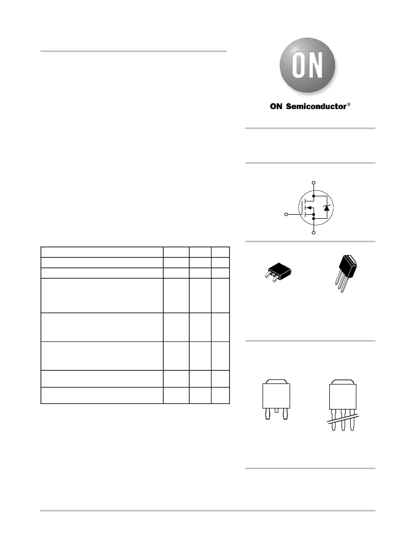
| 封装/外壳: | TO-252-3,DPak(2 引线+接片),SC-63 |
| 供应商设备封装: | DPAK-3 |
| 包装: | 管件 |
| 其它名称: | NTD14N03ROS |
�� �
�
�NTD14N03R,� NVD14N03R�
�Power� MOSFET�
�14� Amps,� 25� Volts�
�N� ?� Channel� DPAK�
�Features�
�?� Planar� HD3e� Process� for� Fast� Switching� Performance�
�?� Low� R� DS(on)� to� Minimize� Conduction� Loss�
�?� Low� C� iss� to� Minimize� Driver� Loss�
�?� Low� Gate� Charge�
�?� Optimized� for� High� Side� Switching� Requirements� in�
�High� ?� Efficiency� DC� ?� DC� Converters�
�?� NVD� Prefix� for� Automotive� and� Other� Applications� Requiring�
�Unique� Site� and� Control� Change� Requirements;� AEC� ?� Q101�
�http://onsemi.com�
�14� AMPERES,� 25� VOLTS�
�R� DS(on)� =� 70.4� m� W� (Typ)�
�N� ?� CHANNEL�
�D�
�?�
�Qualified� and� PPAP� Capable�
�These� Devices� are� Pb� ?� Free� and� are� RoHS� Compliant�
�G�
�S�
�MAXIMUM� RATINGS� (T� J� =� 25� °� C� unless� otherwise� specified)�
�Parameter�
�Drain� ?� to� ?� Source� Voltage�
�Symbol�
�V� DSS�
�Value�
�25�
�Unit�
�Vdc�
�4�
�4�
�Gate� ?� to� ?� Source� Voltage� ?� Continuous�
�Thermal� Resistance� ?� Junction� ?� to� ?� Case�
�Total� Power� Dissipation� @� T� A� =� 25� °� C�
�Drain� Current� ?� Continuous� @� T� A� =� 25� °� C,� Chip�
�?� Continuous� @� T� A� =� 25� °� C,� Limited� by� Package�
�?� Single� Pulse� (tp� ≤� 10� m� s)�
�Thermal� Resistance,� Junction� ?� to� ?� Ambient�
�(Note� 1)�
�Total� Power� Dissipation� @� T� A� =� 25� °� C�
�Drain� Current� ?� Continuous� @� T� A� =� 25� °� C�
�V� GS�
�R� q� JC�
�P� D�
�I� D�
�I� D�
�I� D�
�R� q� JA�
�P� D�
�I� D�
�±� 20�
�6.0�
�20.8�
�14�
�11.4�
�28�
�80�
�1.56�
�3.1�
�Vdc�
�°� C/W�
�W�
�A�
�A�
�A�
�°� C/W�
�W�
�A�
�1� 2�
�3�
�CASE� 369C�
�DPAK�
�(Surface� Mount)�
�STYLE� 2�
�1�
�2�
�3�
�CASE� 369D�
�DPAK� ?� 3�
�(Straight� Lead)�
�STYLE� 2�
�Thermal� Resistance,� Junction� ?� to� ?� Ambient�
�(Note� 2)�
�Total� Power� Dissipation� @� T� A� =� 25� °� C�
�Drain� Current� ?� Continuous� @� T� A� =� 25� °� C�
�R� q� JA�
�P� D�
�I� D�
�120�
�1.04�
�2.5�
�°� C/W�
�W�
�A�
�MARKING� DIAGRAM�
�&� PIN� ASSIGNMENTS�
�Operating� and� Storage� Temperature� Range�
�Maximum� Lead� Temperature� for� Soldering�
�Purposes,� 1/8� ″� from� case� for� 10� seconds�
�T� J� ,� T� stg�
�T� L�
�?� 55� to�
�150�
�260�
�°� C�
�°� C�
�4� Drain�
�4� Drain�
�Source�
�Stresses� exceeding� Maximum� Ratings� may� damage� the� device.� Maximum�
�Ratings� are� stress� ratings� only.� Functional� operation� above� the� Recommended�
�Operating� Conditions� is� not� implied.� Extended� exposure� to� stresses� above� the�
�Recommended� Operating� Conditions� may� affect� device� reliability.�
�1.� When� surface� mounted� to� an� FR4� board� using� 0.5� sq.� in� pad� size.�
�2.� When� surface� mounted� to� an� FR4� board� using� minimum� recommended� pad�
�size.�
�1�
�Gate�
�Y�
�WW�
�3�
�2�
�Drain�
�=� Year�
�=� Work� Week�
�1�
�Gate�
�2�
�Drain�
�3�
�Source�
�14N03�
�G�
�=� Device� Code�
�=� Pb� ?� Free� Package�
�ORDERING� INFORMATION�
�See� detailed� ordering� and� shipping� information� in� the� package�
�dimensions� section� on� page� 5� of� this� data� sheet.�
�?� Semiconductor� Components� Industries,� LLC,� 2012�
�February,� 2012� ?� Rev.� 7�
�1�
�Publication� Order� Number:�
�NTD14N03R/D�
�相关PDF资料 |
PDF描述 |
|---|---|
| RGP10BEHE3/73 | DIODE GPP 1A 100V 150NS DO-41 |
| RCM10DRKI-S13 | CONN EDGECARD 20POS .156 EXTEND |
| PV37X204C01B00 | TRIMMER 200K OHM 0.25W TH |
| EEC22DRXI | CONN EDGECARD 44POS DIP .100 SLD |
| PV37X105C01B00 | TRIMMER 1M OHM 0.25W TH |
相关代理商/技术参数 |
参数描述 |
|---|---|
| NTD14N03R_07 | 制造商:ONSEMI 制造商全称:ON Semiconductor 功能描述:Power MOSFET 14 Amps, 25 Volts N-Channel DPAK |
| NTD14N03R-001 | 功能描述:MOSFET 25V 14A N-Channel RoHS:否 制造商:STMicroelectronics 晶体管极性:N-Channel 汲极/源极击穿电压:650 V 闸/源击穿电压:25 V 漏极连续电流:130 A 电阻汲极/源极 RDS(导通):0.014 Ohms 配置:Single 最大工作温度: 安装风格:Through Hole 封装 / 箱体:Max247 封装:Tube |
| NTD14N03R-1 | 制造商:ONSEMI 制造商全称:ON Semiconductor 功能描述:Power MOSFET 14 Amps, 25 Volts N−Channel DPAK |
| NTD14N03R-1G | 功能描述:MOSFET 25V 14A N-Channel RoHS:否 制造商:STMicroelectronics 晶体管极性:N-Channel 汲极/源极击穿电压:650 V 闸/源击穿电压:25 V 漏极连续电流:130 A 电阻汲极/源极 RDS(导通):0.014 Ohms 配置:Single 最大工作温度: 安装风格:Through Hole 封装 / 箱体:Max247 封装:Tube |
| NTD14N03RG | 功能描述:MOSFET 25V 14A N-Channel RoHS:否 制造商:STMicroelectronics 晶体管极性:N-Channel 汲极/源极击穿电压:650 V 闸/源击穿电压:25 V 漏极连续电流:130 A 电阻汲极/源极 RDS(导通):0.014 Ohms 配置:Single 最大工作温度: 安装风格:Through Hole 封装 / 箱体:Max247 封装:Tube |
发布紧急采购,3分钟左右您将得到回复。