- 您现在的位置:买卖IC网 > Datasheet目录486 > NTD15N06-001 (ON Semiconductor)MOSFET N-CH 60V 15A IPAK Datasheet资料下载
参数资料
| 型号: | NTD15N06-001 |
| 厂商: | ON Semiconductor |
| 文件页数: | 1/8页 |
| 文件大小: | 0K |
| 描述: | MOSFET N-CH 60V 15A IPAK |
| 产品变化通告: | Product Discontinuation 31/Mar/2005 |
| 标准包装: | 75 |
| FET 型: | MOSFET N 通道,金属氧化物 |
| FET 特点: | 标准 |
| 漏极至源极电压(Vdss): | 60V |
| 电流 - 连续漏极(Id) @ 25° C: | 15A |
| 开态Rds(最大)@ Id, Vgs @ 25° C: | 90 毫欧 @ 7.5A,10V |
| Id 时的 Vgs(th)(最大): | 4V @ 250µA |
| 闸电荷(Qg) @ Vgs: | 20nC @ 10V |
| 输入电容 (Ciss) @ Vds: | 450pF @ 25V |
| 功率 - 最大: | 1.5W |
| 安装类型: | 通孔 |
| 封装/外壳: | TO-251-3 短引线,IPak,TO-251AA |
| 供应商设备封装: | I-Pak |
| 包装: | 管件 |
| 其它名称: | NTD15N06-001OS |
��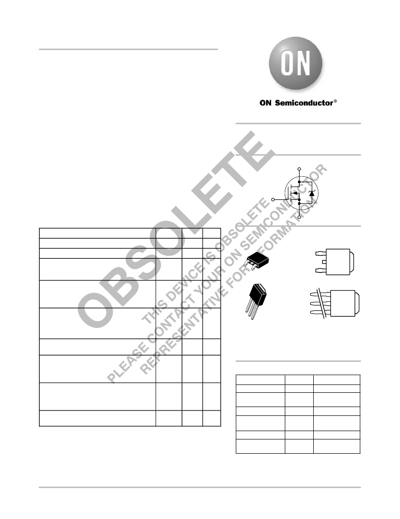 �
�
�NTD15N06�
�Power� MOSFET�
�15� Amps,� 60� Volts�
�N� ?� Channel� DPAK�
�Designed� for� low� voltage,� high� speed� switching� applications� in�
�power� supplies,� converters� and� power� motor� controls� and� bridge�
�circuits.�
�Features�
�?� Pb� ?� Free� Packages� are� Available�
�Applications�
�?� Power� Supplies�
�http://onsemi.com�
�15� AMPERES�
�60� VOLTS�
�R� DS(on)� =� 76� m� W� (� TYP)�
�N� ?� Channel�
�D�
�?�
�Converters�
�?�
�?�
�Power� Motor� Controls�
�Bridge� Circuits�
�G�
�MAXIMUM� RATINGS� (T� J� =� 25� °� C� unless� otherwise� noted)�
�S�
�Rating�
�Drain� ?� to� ?� Source� Voltage�
�Symbol�
�V� DSS�
�Value�
�60�
�Unit�
�Vdc�
�MARKING�
�DIAGRAMS�
�Drain� ?� to� ?� Gate� Voltage� (R� GS� =� 1.0� M� W� )�
�Gate� ?� to� ?� Source� Voltage�
�?� Continuous�
�?� Non� ?� repetitive� (t� p� v� 10� ms)�
�V� DGR�
�V� GS�
�V� GS�
�60�
�"� 20�
�"� 30�
�Vdc�
�Vdc�
�1� 2�
�3�
�4�
�DPAK�
�CASE� 369C�
�STYLE� 2�
�YWW�
�15�
�N06G�
�Drain� Current�
�?� Continuous� @� T� A� =� 25� °� C�
�?� Continuous� @� T� A� =� 100� °� C�
�?� Single� Pulse� (t� p� v� 10� m� s)�
�Total� Power� Dissipation� @� T� J� =� 25� °� C�
�Derate� above� 25� °� C�
�Total� Power� Dissipation� @� T� A� =� 25� °� C� (Note� 1)�
�Total� Power� Dissipation� @� T� A� =� 25� °� C� (Note� 2)�
�I� D�
�I� D�
�I� DM�
�P� D�
�15�
�10�
�45�
�48�
�0.32�
�2.1�
�1.5�
�Adc�
�Apk�
�W�
�W/� °� C�
�W�
�W�
�1�
�2�
�3�
�4�
�15�
�N06�
�DPAK� ?� 3�
�CASE� 369D�
�STYLE� 2�
�=� Device� Code�
�=� Specific� Device�
�YWW�
�15�
�N06G�
�Operating� and� Storage� Temperature� Range�
�Single� Pulse� Drain� ?� to� ?� Source� Avalanche� Ener-�
�gy� ?� Starting� T� J� =� 25� °� C�
�(V� DD� =� 25� Vdc,� V� GS� =� 10� Vdc,� L� =� 1.0� mH,�
�I� L(pk)� =� 11� A,� V� DS� =� 60� Vdc)�
�T� J� ,� T� stg�
�E� AS�
�?� 55� to�
�+175�
�61�
�°� C�
�mJ�
�Y� =� Year�
�W� =� Work� Week�
�G� Pb� ?� Free� Package�
�ORDERING� INFORMATION�
�Device� Package� Shipping� ?�
�Thermal� Resistance� °� C/W�
�?� Junction� ?� to� ?� Case� R� q� JC� 3.13�
�?� Junction� ?� to� ?� Ambient� (Note� 1)� R� q� JA� 71.4�
�?� Junction� ?� to� ?� Ambient� (Note� 2)� R� q� JA� 100�
�Maximum� Lead� Temperature� for� Soldering� Pur-� T� L� 260� °� C�
�poses,� 1/8� ″� from� case� for� 10� seconds�
�Stresses� exceeding� Maximum� Ratings� may� damage� the� device.� Maximum�
�Ratings� are� stress� ratings� only.� Functional� operation� above� the� Recommended�
�Operating� Conditions� is� not� implied.� Extended� exposure� to� stresses� above� the�
�Recommended� Operating� Conditions� may� affect� device� reliability.�
�1.� When� surface� mounted� to� an� FR4� board� using� 0.5� sq� in� pad� size.�
�2.� When� surface� mounted� to� an� FR4� board� using� the� minimum� recommended�
�pad� size.�
�NTD15N06� DPAK� 75� Units� /� Rail�
�NTD15N06G� DPAK� 75� Units� /� Rail�
�(Pb� ?� Free)�
�NTD15N06� ?� 1� DPAK� ?� 3� 75� Units� /� Rail�
�NTD15N06� ?� 1G� DPAK� ?� 3� 75� Units� /� Rail�
�(Pb� ?� Free)�
�NTD15N06T4� DPAK� 2500/Tape� &� Reel�
�NTD15N06T4G� DPAK� 2500/Tape� &� Reel�
�(Pb� ?� Free)�
�?For� information� on� tape� and� reel� specifications,�
�including� part� orientation� and� tape� sizes,� please�
�refer� to� our� Tape� and� Reel� Packaging� Specification�
�Brochure,� BRD8011/D.�
�?� Semiconductor� Components� Industries,� LLC,� 2006�
�August,� 2006� ?� Rev.� 3�
�1�
�Publication� Order� Number:�
�NTD15N06/D�
�相关PDF资料 |
PDF描述 |
|---|---|
| NTD15N06L-001 | MOSFET N-CH 60V 15A IPAK |
| NTD18N06L-001 | MOSFET N-CH 60V 18A IPAK |
| NTD18N06T4G | MOSFET N-CH 60V 18A DPAK |
| NTD20N03L27-001 | MOSFET N-CH 30V 20A IPAK |
| NTD20N06-001 | MOSFET N-CH 60V 20A IPAK |
相关代理商/技术参数 |
参数描述 |
|---|---|
| NTD15N06-1 | 制造商:未知厂家 制造商全称:未知厂家 功能描述:TRANSISTOR | MOSFET | N-CHANNEL | 60V V(BR)DSS | 15A I(D) | TO-252AA |
| NTD15N06AV1 | 制造商:ON Semiconductor 功能描述: |
| NTD15N06AVT4 | 制造商:Rochester Electronics LLC 功能描述:- Bulk |
| NTD15N06L | 制造商:ONSEMI 制造商全称:ON Semiconductor 功能描述:Power MOSFET 15 Amps, 60 Volts, Logic Level |
| NTD15N06L-001 | 功能描述:MOSFET N-CH 60V 15A IPAK RoHS:否 类别:分离式半导体产品 >> FET - 单 系列:- 标准包装:1,000 系列:MESH OVERLAY™ FET 型:MOSFET N 通道,金属氧化物 FET 特点:逻辑电平门 漏极至源极电压(Vdss):200V 电流 - 连续漏极(Id) @ 25° C:18A 开态Rds(最大)@ Id, Vgs @ 25° C:180 毫欧 @ 9A,10V Id 时的 Vgs(th)(最大):4V @ 250µA 闸电荷(Qg) @ Vgs:72nC @ 10V 输入电容 (Ciss) @ Vds:1560pF @ 25V 功率 - 最大:40W 安装类型:通孔 封装/外壳:TO-220-3 整包 供应商设备封装:TO-220FP 包装:管件 |
发布紧急采购,3分钟左右您将得到回复。