- 您现在的位置:买卖IC网 > Datasheet目录486 > NTD15N06L-001 (ON Semiconductor)MOSFET N-CH 60V 15A IPAK Datasheet资料下载
参数资料
| 型号: | NTD15N06L-001 |
| 厂商: | ON Semiconductor |
| 文件页数: | 5/8页 |
| 文件大小: | 0K |
| 描述: | MOSFET N-CH 60V 15A IPAK |
| 产品变化通告: | Product Discontinuation 31/Mar/2005 |
| 标准包装: | 75 |
| FET 型: | MOSFET N 通道,金属氧化物 |
| FET 特点: | 逻辑电平门 |
| 漏极至源极电压(Vdss): | 60V |
| 电流 - 连续漏极(Id) @ 25° C: | 15A |
| 开态Rds(最大)@ Id, Vgs @ 25° C: | 100 毫欧 @ 7.5A,5V |
| Id 时的 Vgs(th)(最大): | 2V @ 250µA |
| 闸电荷(Qg) @ Vgs: | 20nC @ 5V |
| 输入电容 (Ciss) @ Vds: | 440pF @ 25V |
| 功率 - 最大: | 1.5W |
| 安装类型: | 通孔 |
| 封装/外壳: | TO-251-3 短引线,IPak,TO-251AA |
| 供应商设备封装: | I-Pak |
| 包装: | 管件 |
| 其它名称: | NTD15N06L-001OS |
�� �
�
�NTD15N06L�
�6�
�Q� 1�
�Q� T�
�Q� 2�
�1000�
�V� DS� =� 30� V�
�I� D� =� 15� A�
�V� GS� =� 5� V�
�4�
�100�
�t� r�
�2�
�V� GS�
�10�
�t� f�
�t� d(off)�
�t� d(on)�
�0�
�0�
�2� 4�
�6�
�I� D� =� 15� A�
�T� J� =� 25� °� C�
�8�
�1�
�1�
�10�
�100�
�Q� G� ,� TOTAL� GATE� CHARGE� (nC)�
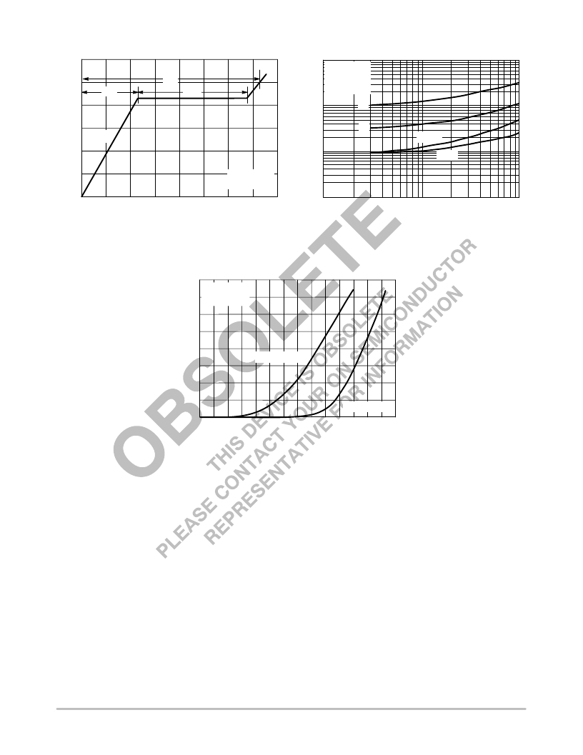
�Figure� 8.� Gate� ?� To� ?� Source� and� Drain� ?� To� ?� Source�
�Voltage� versus� Total� Charge�
�R� G� ,� GATE� RESISTANCE� (� W� )�
�Figure� 9.� Resistive� Switching� Time�
�Variation� versus� Gate� Resistance�
�DRAIN� ?� TO� ?� SOURCE� DIODE� CHARACTERISTICS�
�16�
�12�
�8�
�4�
�V� GS� =� 0� V�
�T� J� =� 25� °� C�
�T� J� =� 150� °� C�
�0�
�0.3�
�0.4�
�0.5�
�0.6�
�0.7�
�0.8�
�T� J� =� 25� °� C�
�0.9�
�1�
�V� SD� ,� SOURCE� ?� TO� ?� DRAIN� VOLTAGE� (VOLTS)�
�Figure� 10.� Diode� Forward� Voltage� versus� Current�
�SAFE� OPERATING� AREA�
�The� Forward� Biased� Safe� Operating� Area� curves� define�
�the� maximum� simultaneous� drain� ?� to� ?� source� voltage� and�
�drain� current� that� a� transistor� can� handle� safely� when� it� is�
�forward� biased.� Curves� are� based� upon� maximum� peak�
�junction� temperature� and� a� case� temperature� (T� C� )� of� 25� °� C.�
�Peak� repetitive� pulsed� power� limits� are� determined� by� using�
�the� thermal� response� data� in� conjunction� with� the� procedures�
�discussed� in� AN569,� “Transient� Thermal� Resistance� ?�
�General� Data� and� Its� Use.”�
�Switching� between� the� off� ?� state� and� the� on� ?� state� may�
�traverse� any� load� line� provided� neither� rated� peak� current�
�(I� DM� )� nor� rated� voltage� (V� DSS� )� is� exceeded� and� the�
�transition� time� (t� r� ,t� f� )� do� not� exceed� 10� m� s.� In� addition� the� total�
�power� averaged� over� a� complete� switching� cycle� must� not�
�exceed� (T� J(MAX)� ?� T� C� )/(R� q� JC� ).�
�A� Power� MOSFET� designated� E� ?� FET� can� be� safely� used�
�in� switching� circuits� with� unclamped� inductive� loads.� For�
�reliable� operation,� the� stored� energy� from� circuit� inductance�
�dissipated� in� the� transistor� while� in� avalanche� must� be� less�
�than� the� rated� limit� and� adjusted� for� operating� conditions�
�differing� from� those� specified.� Although� industry� practice� is�
�to� rate� in� terms� of� energy,� avalanche� energy� capability� is� not�
�a� constant.� The� energy� rating� decreases� non� ?� linearly� with� an�
�increase� of� peak� current� in� avalanche� and� peak� junction�
�temperature.�
�Although� many� E� ?� FETs� can� withstand� the� stress� of�
�drain� ?� to� ?� source� avalanche� at� currents� up� to� rated� pulsed�
�current� (I� DM� ),� the� energy� rating� is� specified� at� rated�
�continuous� current� (I� D� ),� in� accordance� with� industry� custom.�
�The� energy� rating� must� be� derated� for� temperature� as� shown�
�http://onsemi.com�
�5�
�相关PDF资料 |
PDF描述 |
|---|---|
| NTD18N06L-001 | MOSFET N-CH 60V 18A IPAK |
| NTD18N06T4G | MOSFET N-CH 60V 18A DPAK |
| NTD20N03L27-001 | MOSFET N-CH 30V 20A IPAK |
| NTD20N06-001 | MOSFET N-CH 60V 20A IPAK |
| NTD20N06L-001 | MOSFET N-CH 60V 20A IPAK |
相关代理商/技术参数 |
参数描述 |
|---|---|
| NTD15N06L-1 | 制造商:ONSEMI 制造商全称:ON Semiconductor 功能描述:Power MOSFET 15 Amps, 60 Volts, Logic Level |
| NTD15N06L-1G | 制造商:Rochester Electronics LLC 功能描述:- Bulk |
| NTD15N06LG | 制造商:ON Semiconductor 功能描述:Trans MOSFET N-CH 60V 15A 3-Pin(2+Tab) DPAK Rail 制造商:Rochester Electronics LLC 功能描述:- Bulk 制造商:ON Semiconductor 功能描述:MOSFET |
| NTD15N06LT4 | 功能描述:MOSFET N-CH 60V 15A DPAK RoHS:否 类别:分离式半导体产品 >> FET - 单 系列:- 标准包装:1,000 系列:MESH OVERLAY™ FET 型:MOSFET N 通道,金属氧化物 FET 特点:逻辑电平门 漏极至源极电压(Vdss):200V 电流 - 连续漏极(Id) @ 25° C:18A 开态Rds(最大)@ Id, Vgs @ 25° C:180 毫欧 @ 9A,10V Id 时的 Vgs(th)(最大):4V @ 250µA 闸电荷(Qg) @ Vgs:72nC @ 10V 输入电容 (Ciss) @ Vds:1560pF @ 25V 功率 - 最大:40W 安装类型:通孔 封装/外壳:TO-220-3 整包 供应商设备封装:TO-220FP 包装:管件 |
| NTD15N06LT4G | 制造商:Rochester Electronics LLC 功能描述:- Bulk |
发布紧急采购,3分钟左右您将得到回复。